
As depicted in James Bond films, intelligence personnel around the world utilize bugging devices. These devices aid in hearing distant conversations. Their diminutive size enables them to fit in a pocket. They can also be installed in hotel rooms and even within pens.

This design for a bugging device has a range of up to 1 kilometer (or even more). Audio is delivered and received via frequency modulation on both ends. This project requires the components indicated in the bill of materials table.
Hardware Required
- FM Audio Transmitter
- RDA5807M FM Receiver
- Micro Speaker
- ESP8266 12F
- 3.3V Battery
- FTDI Module
- 3D Printed Case
Design
- Transmitter
The used audio transmitter has a mic and three pins, as shown in Figure 2. The transmitter module is powered by a 3.3V rechargeable battery linked to the Vcc and GND pins. The third pin is for connecting the antenna to extend the broadcasting range.
The case used to house the transmitter must contain microscopic holes so that the microphone can catch the sound. In this project, a 3D-printed case was used, which was designed suitably.
- Receiver
The frequency modulation chip RDA5807M is as small as depicted in picture 3. It must be powered by an ESP8266 12F chip, as its I2C communication interface is identical to that of the ESP chip. This scans and matches the receiver’s frequency to that of the broadcast signal. Since the ESP8266 chip lacks USB ports, an FTDI module is required for communication programming. Using the USART serial port to control the RDA5807M FM chip, we send the command to ESP, which then transmits the signal to the FM chip’s I2C port. The radio library is used to drive the FM chip over I2C while creating the program. After installing the ESP board in the Arduino IDE, the ESP chip’s library and programming can be completed.
Once the radio library has been installed in the Arduino IDE, it is uploaded and scanned to the ESP chip. Connecting GPIO 0 to GND and Vcc to 3V on the FTDO module is required to set the ESP chip into programming mode. Before uploading the code, the GND to GND connection coupled with the Tx pin to Rx pin and vice versa must be made.

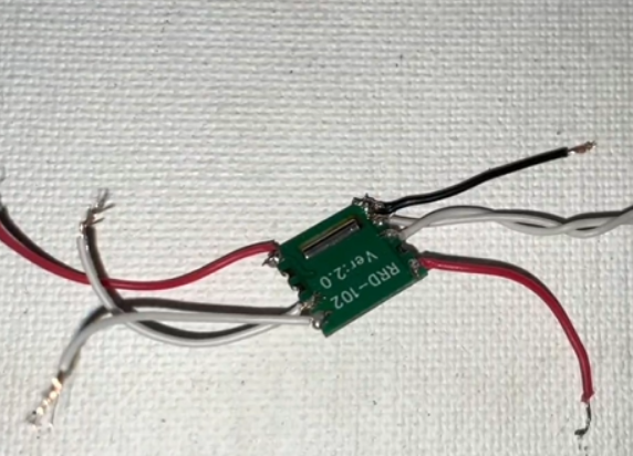
RDA5807M FM chip

Fm receiver connected with the RDA5807M chip.
Connections
After programming the ESP chip, the modules should be connected. The circuit diagram below reveals that the FM audio transmitter module is connected to the battery within the casing.


FM Audio budding transmitter divide fixed inside the case
Next, the appropriate ESP and RDA5807M transmitter chip wires are soldered. The RDA5807M chip’s I2C pins are attached to ESP 12F I2C pins. The powering pins, excluding GND, are attached to the 3V and Vcc pins of ESP. Connecting the antenna to the FM ANT pin of RDA5807M. The L & R audio pins of the RDA5807M are connected to two microspeakers.
RDA5807M wires solderedFig 10. RDA5807M connected with ESP.
Testing

The FM audio transmitter is activated and concealed in the desired area. The serial port is opened and the ESP and FM radio receiver device are connected. After scanning the spectrum of FM channels, the frequency-specific channel is selected. In other words, the FM channel of the audio bugging device has been selected, and you may now hear conversations at the location of the transmitter.
Conclusion
I hope all of you have understood how to design the Smallest FM Audio Bug Spy Device. We MATHA ELECTRONICS will be back soon with more informative blogs soon