
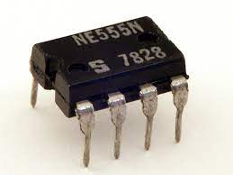
The 555 Timer IC is a popular choice among students and electronics enthusiasts. This IC has a variety of uses, the most common of which are vibrators, such as ASTABLE MULTIVIBRATOR, MONOSTABLE MULTIVIBRATOR, and BISTABLE MULTIVIBRATOR.

This tutorial discusses the various aspects of the 555 Timer IC, and its features, and explains how it works in depth.
What is a 555 Timer IC?
The 555 timer gets its name from the three internally linked 5k resistors that employ to generate the two comparator reference voltages. The 555 timer IC is a low-cost, widely used precision timing device that can be used as a simple timer to generate single pulses or large time delays, or as a relaxation oscillator to generate a string of stabilized waveforms with duty cycles ranging from 50 to 100%.
The IC 555 timer is a single-purpose semiconductor that can be used as an oscillator, pulse generator, or timer. Different electrical and electronic components, such as transistors, resistors, diodes, and a flip flop, can be used to construct IC 555 timers. The operational voltage range of this IC is 4.5V to 15V DC. The 555 timer IC has three working parts: a flip-flop, a voltage divider, and a comparator. This IC’s primary job is to generate a precise timing pulse. The delay of this IC is adjusted by external components such as a resistor and capacitor in monostable mode. Two external resistors and one capacitor control the duty cycle and frequency in the astable mode.
Important Features of the 555 Timer
- Typical operating voltage is +5V, which can withstand a maximum of +18V.
- The source/sink current of the output pin is 200mA
- Consumes up to 3mA when operating at +5V
- Trigger Voltage is 1.67 when operating at +5V
- The operating temperature is 70 degrees Celsius.
- Available in 8-pin PDIP, SOIC, and VSSOP packages
- The o/p of a 555 timer IC can drive TTL due to its high current o/p.
- The timer’s duty cycle is adjustable.
- The max power dissipation per package is 600 milliwatts & its reset and trigger i/ps have logic compatibility.
555 Timer Pin Description

| PIN | NAME | PURPOSE |
| 1 | Ground | Connects the 555 timers to the negative (0v) supply rail |
| 2 | Trigger | Responsible for the transition of the flip-flop from set to reset. The output of the timer depends 2 I on the amplitude of the external trigger pulse applied to this pin |
| 3 | Output | connected to load as it is the only pin with output-driven waveform |
| 4 | Reset | The internal Flip-flop controlling the state of the output, pin 3, is “reset” with this pin. When not in use, this is an active-low input that is usually connected to a logic “1” level to prevent the output from being reset.. |
| 5 | Control voltage | This pin overrides the voltage divider network’s 2/3Vcc level to control the 555’s timing. The width of the output signal can be changed independently of the RC timing network by supplying a voltage to this pin. It is connected to the ground through a 10nF capacitor when not in use to eliminate any noise. |
| 6 | Threshold | The second comparator’s positive input. When the voltage connected to this pin exceeds 2/3Vcc, the Flip-flop is reset, causing the output to transition from “HIGH” to “LOW.” This pin links to the RC timing circuit directly. |
| 7 | Discharge | When the output at pin 3 switches “LOW,” the discharge pin is connected directly to the Collector of an internal NPN transistor, which is used to “discharge” the timing capacitor to the ground. |
| 8 | Supply voltage +Vcc | This is the power supply pin and for general purpose TTL 555 timers are between 4.5V and 15V. |
555 Timer Block Diagram

555 Timer contains a voltage divider network, two comparators, one SR flip-flop, two transistors, and an inverter. This section discusses the purpose of each block or component in detail:
- Three 5k resistors form the voltage divider, which generates two reference voltages. The reference voltages are 1/3 and 2/3 of the supply voltage, which ranges between 5 and 15 volts.
- After that, two comparators compare two analog voltages. The comparator will output 1 if the input voltage at the positive terminal is greater than the input voltage at the negative terminal. Similarly, the comparator will output 0 if the voltage at the negative input terminal is higher than the voltage at the positive terminal.

- The -ve input terminal of the first comparator is connected to the voltage divider’s 2/3 reference voltage and the external control pin, while the +ve input terminal is connected to the external Threshold pin. The -ve input terminal of the second comparator is connected to the Trigger pin, while the +ve input terminal is connected to the voltage divider’s 1/3 reference voltage.
- We can control the output of the two comparators using the three pins Trigger, Threshold, and Control. The output is then sent into the flip-R flops and S inputs. When R is 0 and S is 1, the flip-flop will output 1, and vice versa. The flip-flop can be reset at any moment by using the external pin Reset, which can override the two inputs and reset the entire timer.
The output stage or output drivers receive the Q-bar output of the flip-flip and can either source or sink a current of 200mA to the load. The flip-output flips are also wired to a transistor, which connects the Discharge pin to the ground.
Operating Modes
The 555 generally operates in 3 modes:
- A-stable
- Mono-stable
- Bi-stable modes.
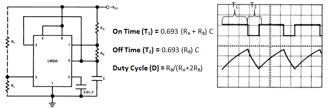
Astable Mode:
The output pin generates a square wave in this mode. This wave is commonly used to switch on and off a load at regular intervals, such as blinking a light. Clock pulse signals for digital ICs are likewise generated in this method. The Resistors (RA, RB) and Capacitor (C) depicted in the diagram below can control the wave’s ON (T1) and OFF (T2) times.
Monostable Mode:
When a trigger button is pressed in Monostable mode, a pre-defined pulse is generated. The output pin is low until the button is pressed, and then it is high for a time determined by the value of the resistor (RA) and capacitor (C) in the circuit below.

Bi-Stable Mode:
Schmitt Trigger Mode is another name for Bi-stable mode. When a load must be turned on and off with a push-button, this mode is employed. This mode is rarely used since it serves no practical use.
Applications
- Time Delay Generation
- Pulse Width Modulation
- Pulse generation
- Precision Timing
- Sequential Timing circuits