
I am text block. Click edit button to change this text. Lorem ipsum dolor sit amet, consectetur adipiscing elit. Ut elit tellus, luctus nec ullamcorper mattis, pulvinar dapibus leo.
-22%

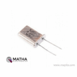
5 MHz 2 Pin Crystal Oscillator
Original price was: ₹35.00.₹25.00Current price is: ₹25.00. inc. GST
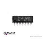
74LS125 Quadruple Bus Buffer IC
Original price was: ₹38.00.₹28.00Current price is: ₹28.00. inc. GST
74LS06 Hex Inverter Buffer Driver IC
Original price was: ₹45.00.₹35.00Current price is: ₹35.00. inc. GST
- Hex Inverter Buffer/Driver
- No. of Gates: 6
- Low Level Output Current: 40mA
- Propagation Delay at 5V: 20ns
- No. of Lines In/Out: 6/6
- Supply Voltage Range: 4.75 to 5.25V
- Package: DIP-14
Description
74LS06 designed as a high-drive, open-collector device used to interface with high-level circuits (such as MOS), or for driving high-current loads. And also are characterized for use as inverter buffers for driving TTL inputs. As a result, this device is perfect for driving multiple inputs and for highspeed applications up to 100 MHz. Meanwhile, 74LS06 devices have rated output voltage of 30 V and a maximum sink current of 40 mA. The 74LS06 widely used for converting TTL voltage levels to MOS levels.
The 74LS06 is a Hex Inverter (NOT gate) integrated circuit. This IC is made up of six NOT gates, each of which has one input and one output pin. That is to say, it is made up of six inverters that conduct logical inverting. An inverter’s output is the inverse of its input logic state, i.e. when the input is high, the output is low, and vice versa. The device consists of six separate gates, each performing the logic INVERT function.
These TTL hex buffers and drivers have high-voltage open-collector outputs, making them excellent for interfacing with high-level circuits (such as MOS) or driving high-current loads (such as lamps or relays). Most TTL families, on the other hand, are completely compatible with these circuits. Furthermore, inputs are diode clamped to decrease transmission-line impacts and simplify construction. This IC has a standard power dissipation of 175 mW and an average propagation latency of 8 ns. A buffer is just a logic gate that passes its input directly to its output. The main goal of a buffer is to regenerate the input signal, which is usually done by using a strong high and a strong low.
Applications
- Factory Automation
- Building Automation
- Line Drivers
- Electronic Point of Sale
- Desktop or Notebook PC
Reviews (0)
Shipping & Delivery

Related products


25pcs Button Switch Kit
- Relative Humidity: 95%
- Rated Voltage: 12V
- Rated Current: 50 mA
- Contact resistance: 50M Ohm Max (initial)
- The insulation resistance: 100M Ohm minDC (250V)
- The compressive strength: AC250V (50/60Hz for 1 minute)
- Mechanical life: 100000 cycles
- The environment temperature: 25° ~ + 105°
- The operating strength: 180/250 (plus or minus 30gf)
- Dimension: 12 * 12 * 7.3 round convex type
- Total Buttons: 25pcs
- Colours: 5 (Black, Red, White, Blue, Yellow)


650NM Laser Diode
- Wavelength: 650nm
- Output optical power: 5mW
- Operating voltage: 5V
- Operating current: ~30mA
- Input current: 30mA
- Housing material: Copper
- Power lead length: 120mm.
- Transmit power: 58mW
- Spot: size 10mm to 15mm at 15meters
- Life span more than 2000 hours
- Driver circuit: APC circuit
- Small size
- Cost-effective
- Breadboard friendly
- Operating temperature -10°C to 40°C
- Dimension: :15mm x 6mm
- Weight: 10 grams
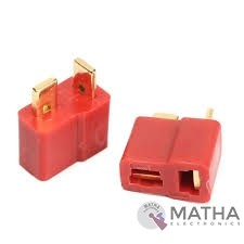
Dean Connector
- Male plug size: About 13* 7* 19mm
- Female plug size: About 13* 7* 15mm
- Current Rating: 30Amps
- Colour: Red and golden
- Material: Plastic and metal
- Provides a secure connection for battery and motor connections
- Eliminates the possibility of wrong polarity connections
- Used in RC hobby, car, boat, plane, helicopter, LIPO battery, etc.
- Dimension: 9x0.7x2cm
- Weight:20gm
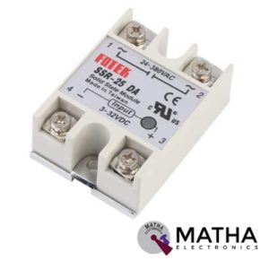
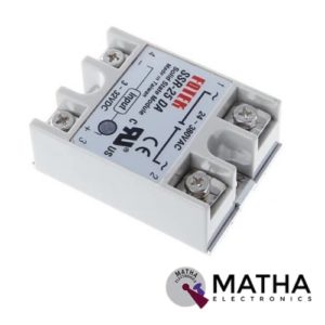
Solid State Relay Module SSR-25DA 25A /250V 3-32V DC Input 24-380VAC Output
- Control mode: DC-AC
- Input voltage: 3-32V DC.
- Output voltage: 24-380V AC.
- Output current: 25A.
- Working voltage: 250V.
- Material: plastic + metal.
- Environment temperature: -30 to +75
- Long service life and high reliability.
- Reduced electromagnetic interference.
- Highly reliable, compact size designed to offer users maximum simplicity.
- Dimension: 6. 5Cm x 4. 5Cm x 2. 2Cm
Reviews
There are no reviews yet.