
I am text block. Click edit button to change this text. Lorem ipsum dolor sit amet, consectetur adipiscing elit. Ut elit tellus, luctus nec ullamcorper mattis, pulvinar dapibus leo.
-33%
")
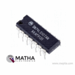
74LS107 Dual J-K Flip-Flop IC
Original price was: ₹30.00.₹25.00Current price is: ₹25.00. inc. GST
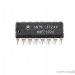
74LS112 Dual J-K Negative Edge Triggered Flip-Flop IC
Original price was: ₹20.00.₹15.00Current price is: ₹15.00. inc. GST
CD4007 Dual Complementary Pair Plus Inverter IC
Original price was: ₹30.00.₹20.00Current price is: ₹20.00. inc. GST
- Dual Complementary Pair Plus Inverter
- DC Supply Voltage Range: −0.5 to +18.0 V
- Input or Output Voltage Range: −0.5 to VDD +0.5 V
- Input or Output Current: ±10 mA
- Power Dissipation: 500 mW
- Low level Output Voltage Max.: 0.05V
- High level Output Voltage: 5.0V
- Low level Input Voltage: 2.25V
- High level Input Voltage: 2.75V
- Propagation Delay Time Max.: 125ns
- Package: DIP-14
Description
The CD4007C designed of three complementary pairs of Nand P-channel enhancement mode MOS transistors. This dual complementary pair transistor is suitable for series/shunt applications. The transistor elements made accessible through the package terminals, As a result, provides a convenient means for constructing the various typical circuits. All inputs protected from static discharge by diode clamps to VDD and VSS. Hence for proper operation, the voltages at all pins must be constrained to be between VSS − 0.3V and VDD + 0.3V at all times.
More complex functions are possible using multiple packages. The CD4007 types manufactured in 14-lead hermetic dual-in-line ceramic packages (F3A suffix), 14-lead dual-in-line plastic packages (E suffix), 14-lead small-outline packages (M, MT, M96, and NSR suffixes), also 14-lead thin shrink small-outline packages (PW and PWR suffixes).
Applications:
- Extremely high-input impedance amplifiers
- Shapers
- Used in inverting operation
- Threshold detector
- Linear amplifiers
- Crystal oscillators
Reviews (0)
Shipping & Delivery

Related products


1/4W 5% Assorted Value Carbon Film Resistor Assortment Kit Set pack electronic diy kit
- 100% brand new and high quality.
- Fine workmanship and long service life.
- 1/4W carbon film resistor package.
- High precision and stability.
- Easy to use.
- Precision: 5%
- Error: 5%
- Values
- 10Ω, 15Ω, 22Ω, 33Ω, 47Ω, 68Ω, 100Ω, 220Ω, 330Ω, 470Ω, 1k, 1k5, 2k2, 3k3, 4k7, 5k6, 6K8, 8K2, 10K, 15K, 22K, 33K, 47K, 56K, 68K, 100K, 150K, 220K, 330K, 470K
- Package included: 150pcs

650NM Laser Diode
- Wavelength: 650nm
- Output optical power: 5mW
- Operating voltage: 5V
- Operating current: ~30mA
- Input current: 30mA
- Housing material: Copper
- Power lead length: 120mm.
- Transmit power: 58mW
- Spot: size 10mm to 15mm at 15meters
- Life span more than 2000 hours
- Driver circuit: APC circuit
- Small size
- Cost-effective
- Breadboard friendly
- Operating temperature -10°C to 40°C
- Dimension: :15mm x 6mm
- Weight: 10 grams


HX711–24 Bit Analog to Digital Converter (ADC)
- It is an ADC converter with two differential input channels
- An active-low noise PGA is integrated inside the chip which provides the gain of 32, 64 and 128
- It has a power-on-reset capability which simplifies digital interface initialization.
- All controls to the IC are made through the pins. Programming is not needed.
- You can select a data rate of 10SPS or 80SPS at the output.
- Provides simultaneous supply rejection of 50Hz and 60Hz supply.
- Built-in analog power supply regulator
- The voltage supply range is from 2.6V to 5.5V
- The temperature range is from -40 °C to +85℃
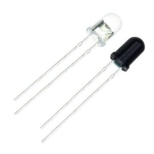
IR LED Sensor
- Size: 5mm LED
- Wavelength: 940nm wavelength (most commonly used)
- Forward current (IF) is 100mA (normal condition) and 300mA (max.)
- 5A of surge forward current
- 24v to 1.4v of forward voltage
- Temperature : -40 to 100 ℃
- Soldering Temperature should not exceed 260 ℃
- Power Dissipation of 150mW at 25℃ (free-air temperature) or below
- Spectral bandwidth of 45nm
- Viewing angle: 30 to 40 degree
- High Reliability
- Excessive radiant intensity
- Having lead spacing of 2.54mm
- Easy to use with breadboard or perf board
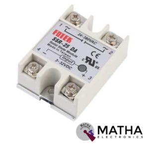
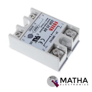
Solid State Relay Module SSR-25DA 25A /250V 3-32V DC Input 24-380VAC Output
- Control mode: DC-AC
- Input voltage: 3-32V DC.
- Output voltage: 24-380V AC.
- Output current: 25A.
- Working voltage: 250V.
- Material: plastic + metal.
- Environment temperature: -30 to +75
- Long service life and high reliability.
- Reduced electromagnetic interference.
- Highly reliable, compact size designed to offer users maximum simplicity.
- Dimension: 6. 5Cm x 4. 5Cm x 2. 2Cm


TP5100 4.2v 8.4v Single Double Lithium Battery Charge Management Li-ion Battery Compatible 2A Charging Board
- Input voltage: 5-15V DC power supply.
- Charge status: full and unloaded blue lights, charging red.
- Double 8.4v / 4.2v lithium rechargeable single .
- Programmable charge current. 0. 1A-2A .
- Programmable steady precharge current 10% -100%.
- Wide operating voltage, maximum reach I8V.
- Red and green LED charge status indicator.
- Chip temperature protection, overcurrent protection, under voltage protection.
- Battery temperature protection, reverse battery shutdown, short circuit protection.
- Switching frequency 400Khz, usable inductance 20uH and more.
- PWR_ON Power battery for switching control.
Reviews
There are no reviews yet.