
I am text block. Click edit button to change this text. Lorem ipsum dolor sit amet, consectetur adipiscing elit. Ut elit tellus, luctus nec ullamcorper mattis, pulvinar dapibus leo.
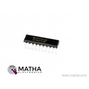
74LS374 Edge-Triggered D Flip-Flop IC
Original price was: ₹23.00.₹18.00Current price is: ₹18.00. inc. GST
CD4099 8-Bit Addressable Latch IC
Original price was: ₹30.00.₹25.00Current price is: ₹25.00. inc. GST
74LS574 Octal Edge Triggered D Flip-Flop IC
- Octal Edge Triggered D Flip-Flop With 3-State Output
- High-level input voltage: 1.5V
- Low-level input voltage: 0.5V
- Input clamp current: ±20mA
- Maximum clock frequency: 5MHz
- Propagation delay time: 265ns
- Supply voltage range: 2 to 6V
- Package: DIP-20
Description
The 74LS574 comes as a part of the 74XXYY IC series. The 74LS574 designed as a high-speed, low-power Octal D-type Flip-Flop featuring separate D-type inputs for every flip-flop. And 3-state outputs for bus-oriented applications. The two sections of the IC controlled independently by the buffered Clock (CP) and Output Enable (OE) control gates provided to all flip-flops in the IC.
The register is fully edge-triggered. The data presented to the D inputs stored within the flip-flops on the LOW-to-HIGH Clock (CP) transition. The state of every D input, one setup time before the Low-to-High clock transitiontransferred to the corresponding flip-flop’s Q output. The 3-State output buffers drive heavily loaded 3-State buses, MOS memories, or MOS microprocessors. Moreover, the active Low Output Enable (OE) controls all eight 3-State buffers independently of the latch operation. Under the condition, when OE is Low, the latched or transparent data appears at the outputs. When OE is High, the outputs are during a high impedance “off” state, which suggests they’re going to neither drive nor load the bus.
A D-type latch/flip-flop with two stable states that is designed as a timed latch. A D-type latch has a one-clock-cycle delay in its input. Delay circuits are frequently produced by cascading multiple D-type flip-flops. This was then used in a variety of applications, such as digital television systems. A D flip-flop, sometimes known as a delay flip-flop, is a D-type flip-flop.
Applications
- Function as a digital building block for a wide variety of temporary data storage & processing devices such as SRAMs & DRAMs etc.
- Also Useful as Input or Output Port for Microprocessors
Reviews (0)
Shipping & Delivery

Related products


650NM Laser Diode
- Wavelength: 650nm
- Output optical power: 5mW
- Operating voltage: 5V
- Operating current: ~30mA
- Input current: 30mA
- Housing material: Copper
- Power lead length: 120mm.
- Transmit power: 58mW
- Spot: size 10mm to 15mm at 15meters
- Life span more than 2000 hours
- Driver circuit: APC circuit
- Small size
- Cost-effective
- Breadboard friendly
- Operating temperature -10°C to 40°C
- Dimension: :15mm x 6mm
- Weight: 10 grams
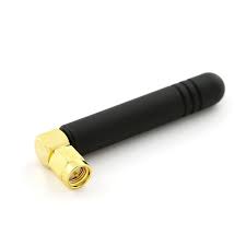
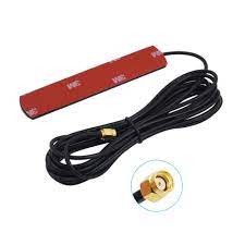
GSM Antenna Dlenp 2dbi/3dbi Patch Antenna with SMA Male Connector
- GSM Antenna
- Gain: 2 to 3dbi
- Wire Length: 3 metre
- 3dbi Sticker Antenna
- GSM Antenna
- SMA Male Connector
- Frequency Range(MHz): 824-960/1710-1990Mhz
- Bandwidth (MHz): 136/280
- VSWR≤1.5
- Gain(dB): 2-3dbi
- Max Input power(W): 60W
- Input Impedance: 50 Ω
- Polarization Type: Vertical
- Cable Type: RG174
- Mounting Adhesive
- Net weight: 47g

HX711–24 Bit Analog to Digital Converter (ADC)
- It is an ADC converter with two differential input channels
- An active-low noise PGA is integrated inside the chip which provides the gain of 32, 64 and 128
- It has a power-on-reset capability which simplifies digital interface initialization.
- All controls to the IC are made through the pins. Programming is not needed.
- You can select a data rate of 10SPS or 80SPS at the output.
- Provides simultaneous supply rejection of 50Hz and 60Hz supply.
- Built-in analog power supply regulator
- The voltage supply range is from 2.6V to 5.5V
- The temperature range is from -40 °C to +85℃

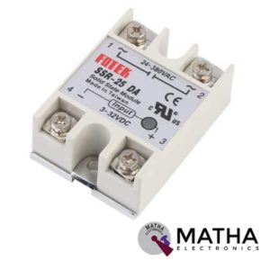
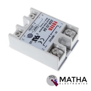
Solid State Relay Module SSR-25DA 25A /250V 3-32V DC Input 24-380VAC Output
- Control mode: DC-AC
- Input voltage: 3-32V DC.
- Output voltage: 24-380V AC.
- Output current: 25A.
- Working voltage: 250V.
- Material: plastic + metal.
- Environment temperature: -30 to +75
- Long service life and high reliability.
- Reduced electromagnetic interference.
- Highly reliable, compact size designed to offer users maximum simplicity.
- Dimension: 6. 5Cm x 4. 5Cm x 2. 2Cm


TP5100 4.2v 8.4v Single Double Lithium Battery Charge Management Li-ion Battery Compatible 2A Charging Board
- Input voltage: 5-15V DC power supply.
- Charge status: full and unloaded blue lights, charging red.
- Double 8.4v / 4.2v lithium rechargeable single .
- Programmable charge current. 0. 1A-2A .
- Programmable steady precharge current 10% -100%.
- Wide operating voltage, maximum reach I8V.
- Red and green LED charge status indicator.
- Chip temperature protection, overcurrent protection, under voltage protection.
- Battery temperature protection, reverse battery shutdown, short circuit protection.
- Switching frequency 400Khz, usable inductance 20uH and more.
- PWR_ON Power battery for switching control.
Reviews
There are no reviews yet.