
I am text block. Click edit button to change this text. Lorem ipsum dolor sit amet, consectetur adipiscing elit. Ut elit tellus, luctus nec ullamcorper mattis, pulvinar dapibus leo.
-14%
")
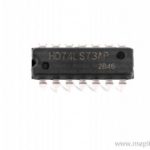
74LS73 Dual Positive Pulse Triggered J-K Flip-Flop IC
Original price was: ₹55.00.₹45.00Current price is: ₹45.00. inc. GST
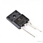
2SK2655 N-Channel Mosfet Transistor 900V 8A
Original price was: ₹200.00.₹150.00Current price is: ₹150.00. inc. GST
74LS75 4-Bit Bistable Latch IC
Original price was: ₹35.00.₹30.00Current price is: ₹30.00. inc. GST
- 4-Bit Bistable Latche
- High-level input voltage: 2V
- Low-level input voltage: 0.8V
- High-level output current: -400µA
- Low-level output current: 8mA
- No. of Circuits: 2
- No. of Inputs: 4
- No. of Outputs: 4
- Input clamp voltage: -1.5V
- Propagation delay time: 30ns
- Supply voltage range: 4.75 to 5.25V
- Package: DIP-16
Description
The 74LS75 are latches used as temporary storage for binary information between processing units and input/output or indicator units. It feature complementary Q and Q’ outputs from a 4-bit latch, and are manufactured in various 16-pin packages. These circuits are perfectly compatible with all popular TTL families. The 74LS75 IC designed to operate at a wide range of working voltage, a wide range of working conditions, and directly interfaces with CMOS, NMOS, and TTL. The output of IC always comes in TTL which makes it easy to figure with other TTL devices and microcontrollers.
When the Enable is HIGH, the Data present at a data (D) input is transferred to the Q output. And the Q output will follow the data input as long as the Enable remains HIGH. Whereas, when the Enable goes LOW, the information (that was present at the data input at the time the transition occurred) is retained at the Q output until the Enable is permitted to go HIGH.
A latch is a device that can be used to store a single bit of data. When the clock input is high, the D latch is used to capture, or ‘latch,’ the logic level existing on the Data line. The output, Q, follows the input, D, if the data on the D line changes state while the clock pulse is high. When the CLK input is set to logic 0, the D input’s last state is trapped and held in the latch.
Applications
- Used in devices such as displays for calculators, digital watches & displays, etc.
- Used in digital clocks, electronic meters, and other electronic devices that display numerical information.
Reviews (0)
Shipping & Delivery

Related products

10 Segment Led Bargraph Light Display Red, Yellow, Green, Blue
- LED type: LED array bar
- Segments: 10
- LED Colour: Green
- Housing color: white
- Reverse voltage: 5V
- Forward Voltage - Typical: 1.85 V
- Forward Voltage - Maximum: 2.2 V
- DC forward current: 30mA
- Peak forward current: 175mA
- Power dissipation: 75mW
- Peak wavelength: 590nm
- Luminous Intensity Typical: 120 Mcd
- Operating temperature: -40°C to +85°C
- 10 Separately Controlled LED's
- High Brightness
- High-Intensity Green Output
- Ideal for Audio and Meter Displays
- Economically priced
- Easy to Mount


5-36v Switch Drive High-power MOSFET Trigger Module
- Operating Voltage: DC 5V - 36V;
- The trigger source: digital high-low (DC3.3V - 20V), can be connected microcontroller IO port, PLC interfaces, DC power, you can access the PWM signal, the signal frequency 0--20KHZ perfect support.
- Output capacity: DC 5V - 36V, at room temperature, continuous current 15A, power 400W! Lower auxiliary cooling conditions, the maximum current up to 30A.
- Applications: You can control the output of power equipment, motors, light bulbs, LED lights, DC motors, micro-pumps, solenoid valves, etc.. You can enter
- PWM, motor speed control, lamp brightness.
- Availability: unlimited switch
- Operating temperature: -40-85
- Dimension: 34mm x 17mm x 12mm
- The use of imported dual-MOS parallel active output, lower resistance, more current, strong power at room temperature, 15A, 400W, to meet the most use of the equipment
- Wide voltage, the perfect support for PWM
- Easily control high power devices
- Input PWM to achieve motor speed control, lamp brightness control

650NM Laser Diode
- Wavelength: 650nm
- Output optical power: 5mW
- Operating voltage: 5V
- Operating current: ~30mA
- Input current: 30mA
- Housing material: Copper
- Power lead length: 120mm.
- Transmit power: 58mW
- Spot: size 10mm to 15mm at 15meters
- Life span more than 2000 hours
- Driver circuit: APC circuit
- Small size
- Cost-effective
- Breadboard friendly
- Operating temperature -10°C to 40°C
- Dimension: :15mm x 6mm
- Weight: 10 grams

HX711–24 Bit Analog to Digital Converter (ADC)
- It is an ADC converter with two differential input channels
- An active-low noise PGA is integrated inside the chip which provides the gain of 32, 64 and 128
- It has a power-on-reset capability which simplifies digital interface initialization.
- All controls to the IC are made through the pins. Programming is not needed.
- You can select a data rate of 10SPS or 80SPS at the output.
- Provides simultaneous supply rejection of 50Hz and 60Hz supply.
- Built-in analog power supply regulator
- The voltage supply range is from 2.6V to 5.5V
- The temperature range is from -40 °C to +85℃
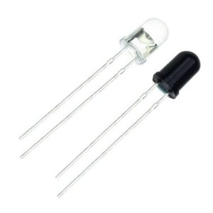
IR LED Sensor
- Size: 5mm LED
- Wavelength: 940nm wavelength (most commonly used)
- Forward current (IF) is 100mA (normal condition) and 300mA (max.)
- 5A of surge forward current
- 24v to 1.4v of forward voltage
- Temperature : -40 to 100 ℃
- Soldering Temperature should not exceed 260 ℃
- Power Dissipation of 150mW at 25℃ (free-air temperature) or below
- Spectral bandwidth of 45nm
- Viewing angle: 30 to 40 degree
- High Reliability
- Excessive radiant intensity
- Having lead spacing of 2.54mm
- Easy to use with breadboard or perf board

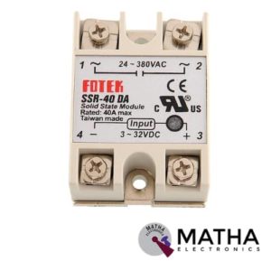
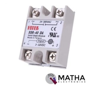
Solid State Relay Module DC To AC SSR-40DA 3-32VDC/24-380VAC 40A
- Control mode: DC-AC
- Input voltage: 3-32V DC.
- Output voltage: 24-380V AC.
- Output current: 40A.
- Working voltage: 250V.
- Material: plastic + metal.
- Loading current: 40A
- Control current: 3-25mA DC
- On voltage: ≤1.5V AC
- One-off Time: ≤10ms
- Off Leakage Current: ≤2mA
- Dielectrics voltage-resistance: 2500VAC
- Environment temperature: -30 to +75
- Long service life and high reliability.
- Reduced electromagnetic interference.
- Highly reliable, compact size designed to offer users maximum simplicity.

Solid State Relay SSR-40DD 40A 3-32V DC to 5-60V DC SSR 40DD Relay Solid State
- Model: SSR-40 DD.
- Control mode: DC-DC
- Input voltage: 3-32V DC.
- Output voltage: 5-60V DC.
- Output current: 40A.
- On voltage: ≤1v.
- One-off time: ≤10ms.
- Off leakage current: ≤2ma.
- Loading current: 40A
- Control current: 3-25mA DC
- Material: plastic + metal.
- Environment temperature: -30 to +75
- Long service life and high reliability.
- Reduced electromagnetic interference.
- Highly reliable, compact size designed to offer users maximum simplicity.
- Weight: 0. 106Kg.
Reviews
There are no reviews yet.