
I am text block. Click edit button to change this text. Lorem ipsum dolor sit amet, consectetur adipiscing elit. Ut elit tellus, luctus nec ullamcorper mattis, pulvinar dapibus leo.
-27%


TL071 Low Noise J-FET Single Operational Amplifier IC
Original price was: ₹48.00.₹30.00Current price is: ₹30.00. inc. GST
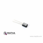
BC327 PNP Transistor -50V -800mA
Original price was: ₹5.00.₹3.00Current price is: ₹3.00. inc. GST
BC177 PNP Transistor 50V 0.1A
Original price was: ₹30.00.₹22.00Current price is: ₹22.00. inc. GST
- Collector-base Voltage: 50V
- Collector Current: 0.1A
- Transistor Polarity: PNP
- Total Power Dissipation: 0.3W
- Transition Frequency: 200MHz
- Current Gain min. : 200 at 2 mA at 5 V, 40 at 10 uA at 5 V
- Package: T0-18
Description
The BC177 designed as a small single NPN Transistor manufactured in TO-18 metal can package. The BC177 comes as a low signal PNP known for its low noise operations making it famously used in signal processing circuits and television receivers. A semiconductor device used to amplify or switch electronic signals and electrical power is classified as BC177. This semiconductor material has at least three terminals for external circuit connection. The current through another pair of terminals is controlled by a voltage or current provided to one pair of transistor terminals. A transistor can magnify a signal because the regulated (output) power can be higher than the controlling (input) power.
Transistors are the most important component in an electrical circuit. A PNP transistor is made up of two pieces of N-type silicon (the base) sandwiched between two pieces of P-type silicon (collector and emitter). The purpose of this transistor was to transfer holes from the emitter to the collector (so conventional current flows from collector to emitter). The emitter “emits” holes into the base, and the quantity of holes the emitter emits is controlled by the base. These holes unite with the electrones in the base and are delivered to the collector. The collector “collects” the majority of the electrons released and transmits them to the next portion of the circuit.
The function of the PNP transistor is to amplify weak signals as they reach the base and create powerful amplified signals at the collector end. The migration of holes in a PNP transistor is from the emitter to the collector area, causing current to flow through the transistor. Because the bulk of charge carriers in such transistors are holes, they have a higher mobility than electrons and are commonly utilised in circuits. The emitter, collector, and base of a PNP transistor are the three terminals. The centre part of a PNP transistor is weakly doped, and it is the most critical factor in the transistor’s operation. Meanwhile, the emitter was little doped, whereas the collector was extensively doped.
Reviews (0)
Shipping & Delivery

Related products


650NM Laser Diode
- Wavelength: 650nm
- Output optical power: 5mW
- Operating voltage: 5V
- Operating current: ~30mA
- Input current: 30mA
- Housing material: Copper
- Power lead length: 120mm.
- Transmit power: 58mW
- Spot: size 10mm to 15mm at 15meters
- Life span more than 2000 hours
- Driver circuit: APC circuit
- Small size
- Cost-effective
- Breadboard friendly
- Operating temperature -10°C to 40°C
- Dimension: :15mm x 6mm
- Weight: 10 grams


ADXL 335 Accelerometer IC
- 3-axis sensing
- Small, low profile package
- 4 mm × 4 mm × 1.45 mm LFCSP
- Low power : 350 μA (typical)
- Single-supply operation: 1.8 V to 3.6 V
- 10,000 g shock survival
- Excellent temperature stability
- BW adjustment with a single capacitor per axis
- RoHS/WEEE lead-free compliant
- 8V- 3.6V single-supply operation
- Integrated X, Y, and Z axis accelerometer on a single chip
- X and Y axis has a 0.5Hz to 1600Hz bandwidth
- Z axis has a 0.5Hz to 550Hz bandwidth
- Hermetically sealed for temp and humidity resistance
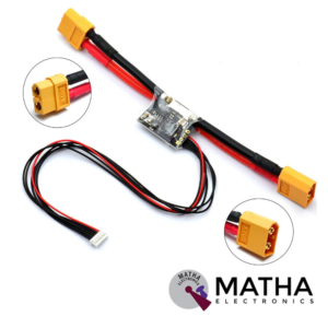
APM/Pixhawk Power Module V6.0 Output BEC 3A XT60 Plug 28V 90A
- Input Voltage Range: 6-28V DC
- Output voltage: 5.3V ± 0.1V
- Maximum output current: 3A
- Maximum current: 90A
- Maximum voltage: 30V
- Supports from 2 cell to 6 cell battery.
- 6P cable can be directly connected to APM/Pixhawk flight control
- Additional 4P rows of pin-free to wire/PIN to connect to another flight control
- Voltage and current measurement configured for 5V ADC.
- Switching regulator outputs 5.3V and 3A max.
- Dimensions: 25mm x 21mm x 9mm
- Weight: 17gm
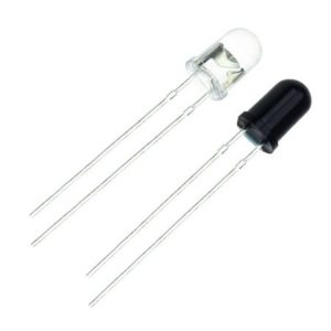
IR LED Sensor
- Size: 5mm LED
- Wavelength: 940nm wavelength (most commonly used)
- Forward current (IF) is 100mA (normal condition) and 300mA (max.)
- 5A of surge forward current
- 24v to 1.4v of forward voltage
- Temperature : -40 to 100 ℃
- Soldering Temperature should not exceed 260 ℃
- Power Dissipation of 150mW at 25℃ (free-air temperature) or below
- Spectral bandwidth of 45nm
- Viewing angle: 30 to 40 degree
- High Reliability
- Excessive radiant intensity
- Having lead spacing of 2.54mm
- Easy to use with breadboard or perf board
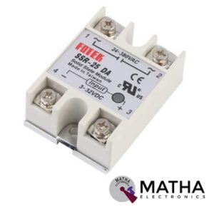
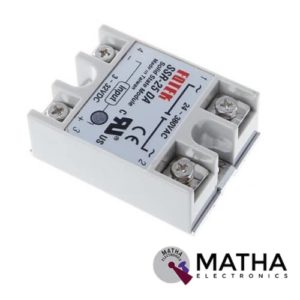
Solid State Relay Module SSR-25DA 25A /250V 3-32V DC Input 24-380VAC Output
- Control mode: DC-AC
- Input voltage: 3-32V DC.
- Output voltage: 24-380V AC.
- Output current: 25A.
- Working voltage: 250V.
- Material: plastic + metal.
- Environment temperature: -30 to +75
- Long service life and high reliability.
- Reduced electromagnetic interference.
- Highly reliable, compact size designed to offer users maximum simplicity.
- Dimension: 6. 5Cm x 4. 5Cm x 2. 2Cm
Reviews
There are no reviews yet.