
I am text block. Click edit button to change this text. Lorem ipsum dolor sit amet, consectetur adipiscing elit. Ut elit tellus, luctus nec ullamcorper mattis, pulvinar dapibus leo.
-24%

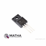
2SK2645 N-Channel Mosfet Transistor 600V 9A
Original price was: ₹95.00.₹85.00Current price is: ₹85.00. inc. GST
CD4027 Dual J-K Master Slave Flip-Flop IC
Original price was: ₹30.00.₹20.00Current price is: ₹20.00. inc. GST
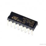
CD4013 Dual D-type Flip-Flop IC
Original price was: ₹33.00.₹25.00Current price is: ₹25.00. inc. GST
- Dual D-type Flip-Flop
- Supply Voltage: 3 to 20V
- Input Current: ± 10 mA
- Power Dissipation: 200mW
- Low level Output Voltage: 0.05V
- High level Output Voltage min.: 4.95V
- Low level Input Voltage Max.: 1.5V
- High level Input Voltage Min.: 3.5V
- Propagation Delay Time Max.: 400ns
- Maximum Clock Frequency: 24MHz
- Package: DIP-14
Description
The CD4013 designed as a CMOS logic chip IC belongs to the CD4XXX IC series. The CD4013 device comprises of two identical, independent data-type flip-flops. Each flip-flop comes with independent data, set, reset, and clock inputs, and Q and Q’ outputs. These devices commonly used for shift register applications, and, by connecting Q output to the data input, for counter and toggle applications. The logic level present at the D input transmitted to the Q output during the positive-going transition of the clock pulse. Moreover, Setting or resetting of IC independent of the clock and accomplished by a high level on the set or reset line, respectively. The CD4013B manufactured in 14-pin dual-inline plastic packages (E suffix), 14-pin small-outline packages (M, MT, M96, and NSR suffixes), and 14-pin thin shrink small-outline packages (PW and PWR suffixes).
A D-type Latch/flip-flop designed as a clocked latch that has two stable states. A D-type latch operates with a delay in input by one clock cycle. Thus, by cascading many D-type flip-flops delay circuits are often created, which are utilized in many applications like in digital television systems. A D-type flip-flop is additionally mentioned as a D flip-flop or a delay flip-flop. The D flip-flop is an edge-triggered device that transfers input file to Q on clock rising or falling edge. Data Latches are level sensitive devices like the data latch and therefore the transparent latch.
Applications
- Power Delivery
- Grid Infrastructure
- Medical, Healthcare, and Fitness
- Body Electronics and Lighting
- Building Automation
- Telecom Infrastructure
- Test and Measurement
Reviews (0)
Shipping & Delivery

Related products


5-36v Switch Drive High-power MOSFET Trigger Module
- Operating Voltage: DC 5V - 36V;
- The trigger source: digital high-low (DC3.3V - 20V), can be connected microcontroller IO port, PLC interfaces, DC power, you can access the PWM signal, the signal frequency 0--20KHZ perfect support.
- Output capacity: DC 5V - 36V, at room temperature, continuous current 15A, power 400W! Lower auxiliary cooling conditions, the maximum current up to 30A.
- Applications: You can control the output of power equipment, motors, light bulbs, LED lights, DC motors, micro-pumps, solenoid valves, etc.. You can enter
- PWM, motor speed control, lamp brightness.
- Availability: unlimited switch
- Operating temperature: -40-85
- Dimension: 34mm x 17mm x 12mm
- The use of imported dual-MOS parallel active output, lower resistance, more current, strong power at room temperature, 15A, 400W, to meet the most use of the equipment
- Wide voltage, the perfect support for PWM
- Easily control high power devices
- Input PWM to achieve motor speed control, lamp brightness control
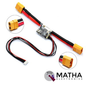
APM/Pixhawk Power Module V6.0 Output BEC 3A XT60 Plug 28V 90A
- Input Voltage Range: 6-28V DC
- Output voltage: 5.3V ± 0.1V
- Maximum output current: 3A
- Maximum current: 90A
- Maximum voltage: 30V
- Supports from 2 cell to 6 cell battery.
- 6P cable can be directly connected to APM/Pixhawk flight control
- Additional 4P rows of pin-free to wire/PIN to connect to another flight control
- Voltage and current measurement configured for 5V ADC.
- Switching regulator outputs 5.3V and 3A max.
- Dimensions: 25mm x 21mm x 9mm
- Weight: 17gm
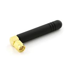
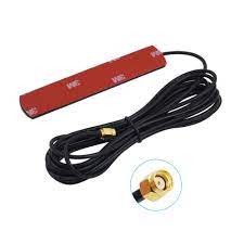
GSM Antenna Dlenp 2dbi/3dbi Patch Antenna with SMA Male Connector
- GSM Antenna
- Gain: 2 to 3dbi
- Wire Length: 3 metre
- 3dbi Sticker Antenna
- GSM Antenna
- SMA Male Connector
- Frequency Range(MHz): 824-960/1710-1990Mhz
- Bandwidth (MHz): 136/280
- VSWR≤1.5
- Gain(dB): 2-3dbi
- Max Input power(W): 60W
- Input Impedance: 50 Ω
- Polarization Type: Vertical
- Cable Type: RG174
- Mounting Adhesive
- Net weight: 47g
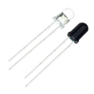
IR LED Sensor
- Size: 5mm LED
- Wavelength: 940nm wavelength (most commonly used)
- Forward current (IF) is 100mA (normal condition) and 300mA (max.)
- 5A of surge forward current
- 24v to 1.4v of forward voltage
- Temperature : -40 to 100 ℃
- Soldering Temperature should not exceed 260 ℃
- Power Dissipation of 150mW at 25℃ (free-air temperature) or below
- Spectral bandwidth of 45nm
- Viewing angle: 30 to 40 degree
- High Reliability
- Excessive radiant intensity
- Having lead spacing of 2.54mm
- Easy to use with breadboard or perf board
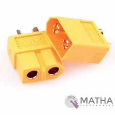
XT60 Connector
- Manufacturer: AMASS
- Connector Series: XT60H
- Rated Voltage: DC 500V
- Metal Material: Brass Gold Plated
- Rated Current: 30A
- Momentary Current: 60A
- Number of pins: 2
- Colour: Yellow
- Contact Resistance: 0.55mΩ
- FR Level: UL94 V0
- Use Times: 1000 TIMES
- Temperature: -20℃ to 120℃
- Spatial Orientation Straight
- Compatible for Wire size up to 12AWG
- Mechanical mounting for cable
- Electrical mounting soldered
- Contact plating Gold flash
Reviews
There are no reviews yet.