
I am text block. Click edit button to change this text. Lorem ipsum dolor sit amet, consectetur adipiscing elit. Ut elit tellus, luctus nec ullamcorper mattis, pulvinar dapibus leo.
-28%
30N60 IGBT 600V 30A
Original price was: ₹200.00.₹180.00Current price is: ₹180.00. inc. GST
CD4049 Hex Buffer or Converter IC
Original price was: ₹20.00.₹15.00Current price is: ₹15.00. inc. GST
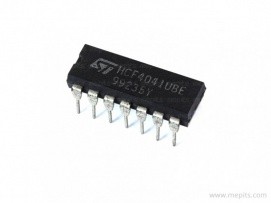
CD4041 Quad True or Complement Buffer IC
Original price was: ₹25.00.₹18.00Current price is: ₹18.00. inc. GST
- Quad True or Complement Buffer
- Supply Voltage Range: 3 to 20V
- Input Current: ±10mA
- Power Dissipation: 200mW
- Low level Output Voltage:0.05V
- High level Output Voltage Min.: 4.95V
- Low level Input Voltage Max.: 1V
- High level Input Voltage Min.: 4V
- Propagation Delay Time Max.: 120ns
- Package: DIP-14
Description
CD4041 made up of monolithic complementary MOS (CMOS) technology, integrated with p-type and n-type enhancement mode transistors. Thus provides a symmetrical circuit with low channel resistance and high current capability supply voltage. The IC also provides buffered outputs which improve transfer characteristics by providing very high gain. In this IC, all the inputs protected against static discharge with diodes to VDD and VSS.
In this, no DC power other than that caused by leakage current consumed during static conditions. Conversion ranges are from 3V to 20V providing VCC ≤ VDD. The devices also have buffered outputs which improve transfer characteristics by providing very high gain.CD4041 hex buffer/converter may be used as ultra-low-power resistor network driver for A/D, D/A converter. Al in the transmission driver and the application where high noise immunity low power dissipation is the primary constraint.
The IC operates a wide range of working conditions, a wide range of operating voltages, and directly interfaces with other hex buffers, CMOS to DTL or TTL interface or as CMOS current drivers. Moreover, CD4041 features high noise immunity and ESD barring. They come with equal source and sink current capabilities and conform to standard B series output drive. The CD4041 IC manufactured in 14 – pin hermetically sealed dual inline package (DIP)ceramic (D) packages. And operates at a voltage ranging from 3V to 20v. CD4041hex buffer/converter may be used as CMOS to TTL or DTL logic-level converters or CMOS
high-sink-current drivers.
APPLICATION
- CMOS to DTL/TTL Hex Converter
- Display Driver
- MOS clock driver
- Resistor network driver
- Transmission line driver
- Buffer
Reviews (0)
Shipping & Delivery

Related products


ADXL 335 Accelerometer IC
- 3-axis sensing
- Small, low profile package
- 4 mm × 4 mm × 1.45 mm LFCSP
- Low power : 350 μA (typical)
- Single-supply operation: 1.8 V to 3.6 V
- 10,000 g shock survival
- Excellent temperature stability
- BW adjustment with a single capacitor per axis
- RoHS/WEEE lead-free compliant
- 8V- 3.6V single-supply operation
- Integrated X, Y, and Z axis accelerometer on a single chip
- X and Y axis has a 0.5Hz to 1600Hz bandwidth
- Z axis has a 0.5Hz to 550Hz bandwidth
- Hermetically sealed for temp and humidity resistance
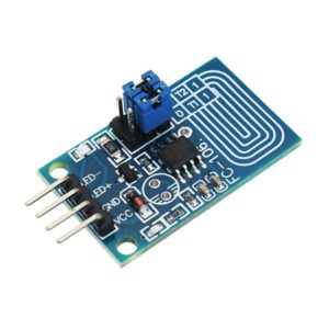
Capacitor Touch Dimmer, Constant Voltage LED Stepless Dimming, PWM Control Board
- Voltage range: 4V to 5V
- Maximum output current: 500mA
- Hole distance: 16 mm
- Aperture: 5 mm
- The lamp brightness can be adjusted by requirement, it is very to operate.
- It can touch in medium protection, such as glass, acrylic, plastic, ceramics, and so on, which is very safe.
- Anti power and phone interference, the EFT can reach above +/-2KV; the touch response sensitivity and reliability will not be affected by the close distance or multi-angle mobile phone interference.
- Dimming mode: Non-polar PWM dimming.
- PCB size: 23 x 20mm
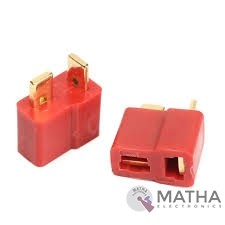
Dean Connector
- Male plug size: About 13* 7* 19mm
- Female plug size: About 13* 7* 15mm
- Current Rating: 30Amps
- Colour: Red and golden
- Material: Plastic and metal
- Provides a secure connection for battery and motor connections
- Eliminates the possibility of wrong polarity connections
- Used in RC hobby, car, boat, plane, helicopter, LIPO battery, etc.
- Dimension: 9x0.7x2cm
- Weight:20gm
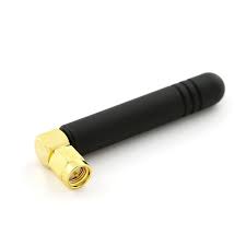

HX711–24 Bit Analog to Digital Converter (ADC)
- It is an ADC converter with two differential input channels
- An active-low noise PGA is integrated inside the chip which provides the gain of 32, 64 and 128
- It has a power-on-reset capability which simplifies digital interface initialization.
- All controls to the IC are made through the pins. Programming is not needed.
- You can select a data rate of 10SPS or 80SPS at the output.
- Provides simultaneous supply rejection of 50Hz and 60Hz supply.
- Built-in analog power supply regulator
- The voltage supply range is from 2.6V to 5.5V
- The temperature range is from -40 °C to +85℃
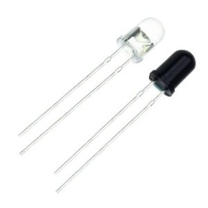
IR LED Sensor
- Size: 5mm LED
- Wavelength: 940nm wavelength (most commonly used)
- Forward current (IF) is 100mA (normal condition) and 300mA (max.)
- 5A of surge forward current
- 24v to 1.4v of forward voltage
- Temperature : -40 to 100 ℃
- Soldering Temperature should not exceed 260 ℃
- Power Dissipation of 150mW at 25℃ (free-air temperature) or below
- Spectral bandwidth of 45nm
- Viewing angle: 30 to 40 degree
- High Reliability
- Excessive radiant intensity
- Having lead spacing of 2.54mm
- Easy to use with breadboard or perf board
Reviews
There are no reviews yet.