
I am text block. Click edit button to change this text. Lorem ipsum dolor sit amet, consectetur adipiscing elit. Ut elit tellus, luctus nec ullamcorper mattis, pulvinar dapibus leo.
-25%

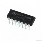
CD4041 Quad True or Complement Buffer IC
Original price was: ₹25.00.₹18.00Current price is: ₹18.00. inc. GST

6 Pin IC Base
Original price was: ₹2.00.₹1.50Current price is: ₹1.50. inc. GST
CD4049 Hex Buffer or Converter IC
Original price was: ₹20.00.₹15.00Current price is: ₹15.00. inc. GST
- Hex Buffer or Converter(Inverting)
- Supply Voltage Range: 3 to 20V
- Input Current: ±10mA
- Power Dissipation: 200mW
- Low level Output Voltage: 0.05V
- High level Output Voltage Min.: 4.95V
- Low level Input Voltage Max.: 1V
- High level Input Voltage Min.: 4V
- Propagation Delay Time Max.: 120ns
- Package: DIP-16
Description
CD4049 designed as a Hex Inverter (NOT gate) IC-based on monolithic complementary MOS (CMOS) technology. This IC come with six NOT gates inside it and each gate provide one input and one output pin. All six NOT gates powered with a common rail, but can operate independently. This Converter IC widely used in buffer circuits and wave generator circuits. The CD4049 has an inverted hex buffer and supports logic-level conversion with just one supply voltage (VCC). The input-signal high level (VIH) can surpass the VCC supply voltage when these devices are utilized for logic-level conversions. These devices designed explicitly for use as CMOS to DTL or TTL converters and drive directly two DTL or TTL loads. (VCC = 5 V, VOL ≤ 0.4 V, and IOL ≥ 3.3 mA.)
The CD4049 offers a wide operating voltage range of 3V to 18V, making it ideal for high voltage applications. Because it’s an inverter IC, it converts logic levels from HIGH to LOW and LOW to HIGH. As a result, it’s commonly employed in logic-level conversions. A voltage greater than 18V may harm the IC in some circumstances. In general, the CD4049 IC is employed in situations where the operation is dependent on one of two states: 0 or 1. For instance, basic LED torches, automated streetlights, and so forth. Simple toggling circuits, voltage multiplier circuits, and a square wave oscillator circuit all employ this component. It can also be used to reverse the output.
CD4049 IC Applications
- CMOS to DTL or TTL Hex Converters
- CMOS Current Sink or Source Drivers
- CMOS High-to-Low Logic Level Converters
Reviews (0)
Shipping & Delivery

Related products

650NM Laser Diode
- Wavelength: 650nm
- Output optical power: 5mW
- Operating voltage: 5V
- Operating current: ~30mA
- Input current: 30mA
- Housing material: Copper
- Power lead length: 120mm.
- Transmit power: 58mW
- Spot: size 10mm to 15mm at 15meters
- Life span more than 2000 hours
- Driver circuit: APC circuit
- Small size
- Cost-effective
- Breadboard friendly
- Operating temperature -10°C to 40°C
- Dimension: :15mm x 6mm
- Weight: 10 grams

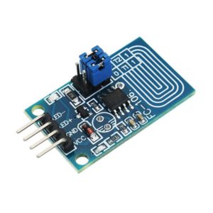
Capacitor Touch Dimmer, Constant Voltage LED Stepless Dimming, PWM Control Board
- Voltage range: 4V to 5V
- Maximum output current: 500mA
- Hole distance: 16 mm
- Aperture: 5 mm
- The lamp brightness can be adjusted by requirement, it is very to operate.
- It can touch in medium protection, such as glass, acrylic, plastic, ceramics, and so on, which is very safe.
- Anti power and phone interference, the EFT can reach above +/-2KV; the touch response sensitivity and reliability will not be affected by the close distance or multi-angle mobile phone interference.
- Dimming mode: Non-polar PWM dimming.
- PCB size: 23 x 20mm


Dual Micro USB 3.7v to 5V 2A Power Bank DIY 18650 LiPo Charger
- 4-level LED lamp display power, not working state intelligent automatic shutdown;
- The built-in lithium battery protection IC, over-current, under-voltage protection;
- Dual USB output ports.
- Dimensions: 68 x 34 x 9 mm (LxWxH)
- Weight: 10 gm
- Input port: MicroUSB (Andro)
- Input requirements: 5V constant voltage power supply can do charge input power, the most matching charger for 5v1a above
- Output port: USB
- Output parameters: 5V1A/5V2A
- Requirements for rechargeable batteries:
- Compatible Batteries: 18650 batteries, cell phone batteries, flat-panel batteries, MP3 batteries, etc. 3.7v-4.2V polymer Lithium battery,
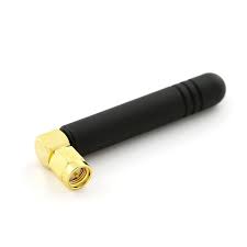
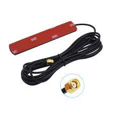
GSM Antenna Dlenp 2dbi/3dbi Patch Antenna with SMA Male Connector
- GSM Antenna
- Gain: 2 to 3dbi
- Wire Length: 3 metre
- 3dbi Sticker Antenna
- GSM Antenna
- SMA Male Connector
- Frequency Range(MHz): 824-960/1710-1990Mhz
- Bandwidth (MHz): 136/280
- VSWR≤1.5
- Gain(dB): 2-3dbi
- Max Input power(W): 60W
- Input Impedance: 50 Ω
- Polarization Type: Vertical
- Cable Type: RG174
- Mounting Adhesive
- Net weight: 47g

HX711–24 Bit Analog to Digital Converter (ADC)
- It is an ADC converter with two differential input channels
- An active-low noise PGA is integrated inside the chip which provides the gain of 32, 64 and 128
- It has a power-on-reset capability which simplifies digital interface initialization.
- All controls to the IC are made through the pins. Programming is not needed.
- You can select a data rate of 10SPS or 80SPS at the output.
- Provides simultaneous supply rejection of 50Hz and 60Hz supply.
- Built-in analog power supply regulator
- The voltage supply range is from 2.6V to 5.5V
- The temperature range is from -40 °C to +85℃
Reviews
There are no reviews yet.