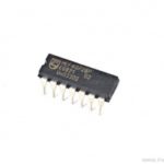
CD4071 comprises four independent OR gates manufactured inside the single integrated circuit package with each OR gate supporting two inputs. The CD4071 designed with complementary MOS (CMOS) transistors technology. It helps to acheive a wide power supply operating range, low power consumption, and high noise margin. The CD4071B manufactured in 14-lead hermetic dual-in-line ceramic packages perfect for use in low power applications.
Meanwhile, the CD4071 employs basic functions required in the implementation of digital integrated circuit systems. The N- and P channel enhancement mode transistors offer a symmetrical circuit with an output swing essentially equivalent to the supply voltage. They features equal source and sink current capabilities and conform to standard B series output drive. The devices also consists of buffered outputs that improve transfer characteristics by providing very high gain. All inputs protected against static discharge with diodes to VDD and VSS.
Moreover, this IC allows design engineers to direct implementation of the positive-logic OR function and supplement the existing family of CMOS gates. CD4071 features high noise immunity and static protection through clamping diodes. The IC designed to operates at 5V, 10V, 15V, and even 20V. While operating at 5V, it offers a maximum low-level input voltage of 0.5V and the minimum high-level input voltage of 4.5V.
An OR gate designed as a logic gate that performs logical OR operation. A logical OR operation consists of a high output (1) if one or both the inputs to the gate remains high (1). In case, if neither input is high, a low output (0) results.
APPLICATIONS
- Used in designing basic logic circuits or Alarm circuits such as alarm for a car door system designed using this IC.
- Encoder
- Decoders
- We can design Multiplexers of any size and also De-multiplexers


Reviews
There are no reviews yet.