
I am text block. Click edit button to change this text. Lorem ipsum dolor sit amet, consectetur adipiscing elit. Ut elit tellus, luctus nec ullamcorper mattis, pulvinar dapibus leo.
-19%
")
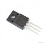
8N60 N-Channel Power Mosfet Transistor 600V 7.5A
Original price was: ₹73.00.₹65.00Current price is: ₹65.00. inc. GST
CD4075BE CMOS OR Gate IC
Original price was: ₹30.00.₹20.00Current price is: ₹20.00. inc. GST
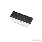
CD4073 Triple 3 Input AND Gate IC
Original price was: ₹31.00.₹25.00Current price is: ₹25.00. inc. GST
- Triple 3 Input AND Gate
- No Of Inputs: 9
- No Of Outputs: 3
- Supply Voltage Range: 3 to 15V
- Quiescent Current Max.: 4µA
- Propagation Delay Time Max.: 110ns
- Package: DIP-14
Description
CD4073 belong to the CD4XXX IC series. This CD4073 designed as monolithic Triple 3-input AND Gate designed by implementing the complementary MOS technology, integrated with P and N type enhancement mode transistors. . The CD4073 IC operates at a wide range of working voltage, a wide range of working conditions. And directly interfaces with CMOS, NMOS, and TTL. The output of the IC always comes in TTL which makes it quite easy to function with other TTL devices and microcontrollers.
ESD blocking and excellent noise immunity are among the properties of CD4073. Clamping diodes were used to safeguard each output from static harm. The supply voltage for the CD4073 is between 3 and 15 volts. This IC is designed to work in the whole military temperature range of 0 to 70 degrees Celsius. The IC CD4073 is smaller in size and has a significantly faster speed, making it extremely reliable in any device. The CD4073 IC can be directly connected to the circuit board or put on a 14-pin IC base. The CD4073 manufactured in 14-lead hermetic dual-in-line ceramic packages (F3A suffix), 14-lead dual-in-line plastic packages (E suffix), 14-lead small-outline packages (M, MT, M96, and NSR suffixes), and 14-lead thin shrink small-outline packages (PW and PWR suffixes).
The AND gate is a simple digital logic gate that performs logical conjunction. The logic multiplication rules are used to operate an AND gate. If all of the AND gate’s inputs are HIGH, the output will also be HIGH. The AND gate produces a LOW output if none or only some of the inputs are HIGH.
Application
- Measurement of frequency
- Enable gate and Inhibit gate
Reviews (0)
Shipping & Delivery

Related products

25pcs Button Switch Kit
- Relative Humidity: 95%
- Rated Voltage: 12V
- Rated Current: 50 mA
- Contact resistance: 50M Ohm Max (initial)
- The insulation resistance: 100M Ohm minDC (250V)
- The compressive strength: AC250V (50/60Hz for 1 minute)
- Mechanical life: 100000 cycles
- The environment temperature: 25° ~ + 105°
- The operating strength: 180/250 (plus or minus 30gf)
- Dimension: 12 * 12 * 7.3 round convex type
- Total Buttons: 25pcs
- Colours: 5 (Black, Red, White, Blue, Yellow)


HX711–24 Bit Analog to Digital Converter (ADC)
- It is an ADC converter with two differential input channels
- An active-low noise PGA is integrated inside the chip which provides the gain of 32, 64 and 128
- It has a power-on-reset capability which simplifies digital interface initialization.
- All controls to the IC are made through the pins. Programming is not needed.
- You can select a data rate of 10SPS or 80SPS at the output.
- Provides simultaneous supply rejection of 50Hz and 60Hz supply.
- Built-in analog power supply regulator
- The voltage supply range is from 2.6V to 5.5V
- The temperature range is from -40 °C to +85℃

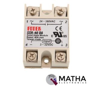
Solid State Relay Module DC To AC SSR-40DA 3-32VDC/24-380VAC 40A
- Control mode: DC-AC
- Input voltage: 3-32V DC.
- Output voltage: 24-380V AC.
- Output current: 40A.
- Working voltage: 250V.
- Material: plastic + metal.
- Loading current: 40A
- Control current: 3-25mA DC
- On voltage: ≤1.5V AC
- One-off Time: ≤10ms
- Off Leakage Current: ≤2mA
- Dielectrics voltage-resistance: 2500VAC
- Environment temperature: -30 to +75
- Long service life and high reliability.
- Reduced electromagnetic interference.
- Highly reliable, compact size designed to offer users maximum simplicity.
Reviews
There are no reviews yet.