
I am text block. Click edit button to change this text. Lorem ipsum dolor sit amet, consectetur adipiscing elit. Ut elit tellus, luctus nec ullamcorper mattis, pulvinar dapibus leo.
-33%


TEA2025 Stereo Audio Amplifier IC
Original price was: ₹45.00.₹35.00Current price is: ₹35.00. inc. GST
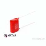
470nf 400V DC Polyester Capacitor
Original price was: ₹20.00.₹5.00Current price is: ₹5.00. inc. GST
CD4093 Quad 2-Input NAND Schmitt Trigger IC
Original price was: ₹30.00.₹20.00Current price is: ₹20.00. inc. GST
- Quad 2-input NAND Schmitt trigger
- Logic IC Family: 4000 CMOS
- Propagation Delay Time: 80 ns
- Number of Lines In/Out: 8 / 4
- Output Current: 2.4mA
- No. of Pins: 14
- No. of Gates: 4
- Output Current Max: 3.4mA
- Operating Temperature Range: -40°C to +70°C
- Supply Voltage Range: 4.5V to 15.5V
- Package: DIP-14
Description
CD4093 is part of the CD4000 IC family. Each of the four Schmitt trigger circuits in the CD4093 IC operates as a two-input NAND logic gate. For positive and negative-going signals, the gate changes at various places. Hysteresis voltage is the difference between the positive (VT+) and negative (VT) voltages (VH). ESD protection, low thermal dissipation, and input diode clamps are also included in this IC (in order to protect the input pins from damage caused by any static discharge).
A Schmitt Trigger is a comparator-based circuit that produces an output based on the output of the prior gate. The input value of a Schmitt Trigger might be analogue or digital, but the output is always in one of two forms: 1 or 0. Any circuit may be converted to Schmitt trigger by using a positive feedback scheme. The threshold utilised to get the output of a Schmitt Trigger circuit, on the other hand. The output remains HIGH when the value exceeds the threshold. It will be deemed in the LOW condition otherwise. Not only are these circuits used to convert analogue to digital, but they also assist reduce noise from the signal.
The NAND gate is a type of digital logic gate that is frequently utilised in DLD applications. It’s also known as a universal logic gate since it may be used to build any logic gate or expression. If any of the NAND gate’s inputs are set to high, the gate’s output will always be a logical low. A NAND gate, on the other hand, produces a logical high only when all of its inputs are set to LOW.
Application
- Wave and pulse shapers
- High-noise-environment systems
- Monostable multivibrators
- Astable multivibrators
- NAND logic
Reviews (0)
Shipping & Delivery

Related products

25pcs Button Switch Kit
- Relative Humidity: 95%
- Rated Voltage: 12V
- Rated Current: 50 mA
- Contact resistance: 50M Ohm Max (initial)
- The insulation resistance: 100M Ohm minDC (250V)
- The compressive strength: AC250V (50/60Hz for 1 minute)
- Mechanical life: 100000 cycles
- The environment temperature: 25° ~ + 105°
- The operating strength: 180/250 (plus or minus 30gf)
- Dimension: 12 * 12 * 7.3 round convex type
- Total Buttons: 25pcs
- Colours: 5 (Black, Red, White, Blue, Yellow)

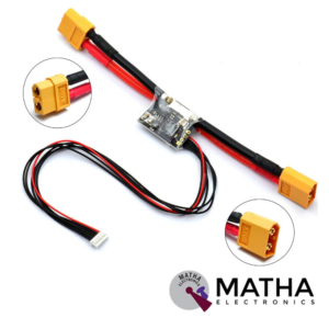
APM/Pixhawk Power Module V6.0 Output BEC 3A XT60 Plug 28V 90A
- Input Voltage Range: 6-28V DC
- Output voltage: 5.3V ± 0.1V
- Maximum output current: 3A
- Maximum current: 90A
- Maximum voltage: 30V
- Supports from 2 cell to 6 cell battery.
- 6P cable can be directly connected to APM/Pixhawk flight control
- Additional 4P rows of pin-free to wire/PIN to connect to another flight control
- Voltage and current measurement configured for 5V ADC.
- Switching regulator outputs 5.3V and 3A max.
- Dimensions: 25mm x 21mm x 9mm
- Weight: 17gm
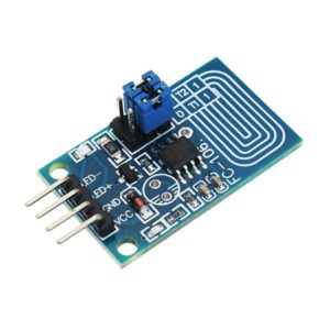
Capacitor Touch Dimmer, Constant Voltage LED Stepless Dimming, PWM Control Board
- Voltage range: 4V to 5V
- Maximum output current: 500mA
- Hole distance: 16 mm
- Aperture: 5 mm
- The lamp brightness can be adjusted by requirement, it is very to operate.
- It can touch in medium protection, such as glass, acrylic, plastic, ceramics, and so on, which is very safe.
- Anti power and phone interference, the EFT can reach above +/-2KV; the touch response sensitivity and reliability will not be affected by the close distance or multi-angle mobile phone interference.
- Dimming mode: Non-polar PWM dimming.
- PCB size: 23 x 20mm

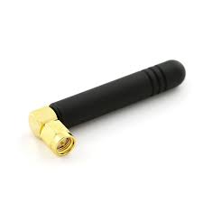

HX711–24 Bit Analog to Digital Converter (ADC)
- It is an ADC converter with two differential input channels
- An active-low noise PGA is integrated inside the chip which provides the gain of 32, 64 and 128
- It has a power-on-reset capability which simplifies digital interface initialization.
- All controls to the IC are made through the pins. Programming is not needed.
- You can select a data rate of 10SPS or 80SPS at the output.
- Provides simultaneous supply rejection of 50Hz and 60Hz supply.
- Built-in analog power supply regulator
- The voltage supply range is from 2.6V to 5.5V
- The temperature range is from -40 °C to +85℃

Reviews
There are no reviews yet.