
I am text block. Click edit button to change this text. Lorem ipsum dolor sit amet, consectetur adipiscing elit. Ut elit tellus, luctus nec ullamcorper mattis, pulvinar dapibus leo.
-47%


2N6288 NPN Transistor 40V 7A
Original price was: ₹28.00.₹20.00Current price is: ₹20.00. inc. GST
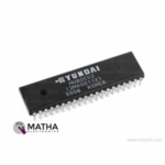
80C52 Microcontroller IC
Original price was: ₹80.00.₹60.00Current price is: ₹60.00. inc. GST
2N3906 PNP Transistor 40V 0.2A
Original price was: ₹7.50.₹4.00Current price is: ₹4.00. inc. GST
- Collector-base Voltage: 40V
- Collector Current: 0.2A
- Transistor Polarity: PNP
- Total Power Dissipation: 0.625W
- Current Gain: 100 at 10 mA at 1 V
- Transition Frequency: 250MHz
- Package: T0-92
Description
2N3906 PNP Transistor 40V 0.2A designed a Bi-Polar PNP Transistor that comes in TO-92 package at 7 A Continuous Collector Current. This three-layer PNP transistor is intended for use in linear applications such as power audio, disc head positioners, and switching. The base current IB determines the collector current IC. For a given collector emitter voltage VCE, every change in the base current causes an amplified change in the collector current.
Transistors are the most important component in an electrical circuit. A PNP transistor is made up of two pieces of N-type silicon (the base) sandwiched between two pieces of P-type silicon (collector and emitter). The purpose of this transistor was to transfer holes from the emitter to the collector (so conventional current flows from collector to emitter). The emitter “emits” holes into the base, and the quantity of holes the emitter emits is controlled by the base. These holes unite with the electrones in the base and are delivered to the collector. The collector “collects” the majority of the electrons released and transmits them to the next portion of the circuit.
The function of the PNP transistor is to amplify weak signals as they reach the base and create powerful amplified signals at the collector end. The migration of holes in a PNP transistor is from the emitter to the collector area, causing current to flow through the transistor. Because the bulk of charge carriers in such transistors are holes, which have a higher mobility than electrons, they are commonly utilised in circuits. The emitter, collector, and base of a PNP transistor are the three terminals. The centre part of a PNP transistor is weakly doped, and it is the most critical factor in the transistor’s operation. Meanwhile, the emitter was little doped, whereas the collector was extensively doped.
Reviews (0)
Shipping & Delivery

Related products
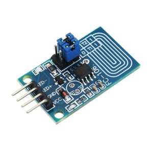
Capacitor Touch Dimmer, Constant Voltage LED Stepless Dimming, PWM Control Board
- Voltage range: 4V to 5V
- Maximum output current: 500mA
- Hole distance: 16 mm
- Aperture: 5 mm
- The lamp brightness can be adjusted by requirement, it is very to operate.
- It can touch in medium protection, such as glass, acrylic, plastic, ceramics, and so on, which is very safe.
- Anti power and phone interference, the EFT can reach above +/-2KV; the touch response sensitivity and reliability will not be affected by the close distance or multi-angle mobile phone interference.
- Dimming mode: Non-polar PWM dimming.
- PCB size: 23 x 20mm


Dual Micro USB 3.7v to 5V 2A Power Bank DIY 18650 LiPo Charger
- 4-level LED lamp display power, not working state intelligent automatic shutdown;
- The built-in lithium battery protection IC, over-current, under-voltage protection;
- Dual USB output ports.
- Dimensions: 68 x 34 x 9 mm (LxWxH)
- Weight: 10 gm
- Input port: MicroUSB (Andro)
- Input requirements: 5V constant voltage power supply can do charge input power, the most matching charger for 5v1a above
- Output port: USB
- Output parameters: 5V1A/5V2A
- Requirements for rechargeable batteries:
- Compatible Batteries: 18650 batteries, cell phone batteries, flat-panel batteries, MP3 batteries, etc. 3.7v-4.2V polymer Lithium battery,

HX711–24 Bit Analog to Digital Converter (ADC)
- It is an ADC converter with two differential input channels
- An active-low noise PGA is integrated inside the chip which provides the gain of 32, 64 and 128
- It has a power-on-reset capability which simplifies digital interface initialization.
- All controls to the IC are made through the pins. Programming is not needed.
- You can select a data rate of 10SPS or 80SPS at the output.
- Provides simultaneous supply rejection of 50Hz and 60Hz supply.
- Built-in analog power supply regulator
- The voltage supply range is from 2.6V to 5.5V
- The temperature range is from -40 °C to +85℃

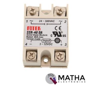
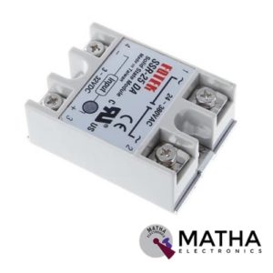
Solid State Relay Module DC To AC SSR-40DA 3-32VDC/24-380VAC 40A
- Control mode: DC-AC
- Input voltage: 3-32V DC.
- Output voltage: 24-380V AC.
- Output current: 40A.
- Working voltage: 250V.
- Material: plastic + metal.
- Loading current: 40A
- Control current: 3-25mA DC
- On voltage: ≤1.5V AC
- One-off Time: ≤10ms
- Off Leakage Current: ≤2mA
- Dielectrics voltage-resistance: 2500VAC
- Environment temperature: -30 to +75
- Long service life and high reliability.
- Reduced electromagnetic interference.
- Highly reliable, compact size designed to offer users maximum simplicity.
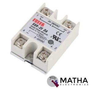
Solid State Relay Module SSR-25DA 25A /250V 3-32V DC Input 24-380VAC Output
- Control mode: DC-AC
- Input voltage: 3-32V DC.
- Output voltage: 24-380V AC.
- Output current: 25A.
- Working voltage: 250V.
- Material: plastic + metal.
- Environment temperature: -30 to +75
- Long service life and high reliability.
- Reduced electromagnetic interference.
- Highly reliable, compact size designed to offer users maximum simplicity.
- Dimension: 6. 5Cm x 4. 5Cm x 2. 2Cm


TP5100 4.2v 8.4v Single Double Lithium Battery Charge Management Li-ion Battery Compatible 2A Charging Board
- Input voltage: 5-15V DC power supply.
- Charge status: full and unloaded blue lights, charging red.
- Double 8.4v / 4.2v lithium rechargeable single .
- Programmable charge current. 0. 1A-2A .
- Programmable steady precharge current 10% -100%.
- Wide operating voltage, maximum reach I8V.
- Red and green LED charge status indicator.
- Chip temperature protection, overcurrent protection, under voltage protection.
- Battery temperature protection, reverse battery shutdown, short circuit protection.
- Switching frequency 400Khz, usable inductance 20uH and more.
- PWR_ON Power battery for switching control.
Reviews
There are no reviews yet.