
A Complete Guide on 8051 Microcontroller Memory Organization
In this tutorial, we will discuss the 8051 microcontrollers by learning how its program memory (ROM), data memory (RAM), and external memory are organized.
The key distinction between a microprocessor and a microcontroller that was made in the previous course was that the former contains both program memory (ROM) and data memory (RAM) on the same chip (IC), whilst the latter requires an external interface to connect to memory modules.
It is therefore evident that memory is a crucial component of the 8051 Microcontroller Architecture (for that matter, any Microcontroller). Therefore, it is crucial for us to comprehend how the memory on an 8051 microcontroller is organized, how the processor accesses each memory, and how to connect external memory to the microcontroller.
Before delving into the specifics of the 8051 Microcontroller Memory Structure, we will first briefly discuss computer architecture before moving on to the 8051 Microcontroller memory organization.
Types of Computer Architecture
Basically, Microprocessors or Microcontrollers are classified based on the two types of Computer Architecture: Von Neumann Architecture and Harvard Architecture.
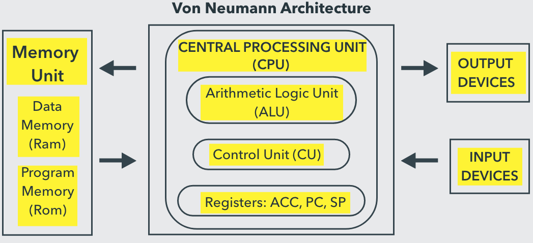
Von Neumann Architecture
The Princeton or Von Neumann architecture of computers stores both the program—that is, the instructions and the data—in a single memory.
The Processor or CPU cannot access both Instructions and Data at the same time since they use a single bus because the Instruction Memory and the Data Memory are the same.
This kind of architecture severely restricts the system’s performance because it causes a bottleneck while accessing memory.
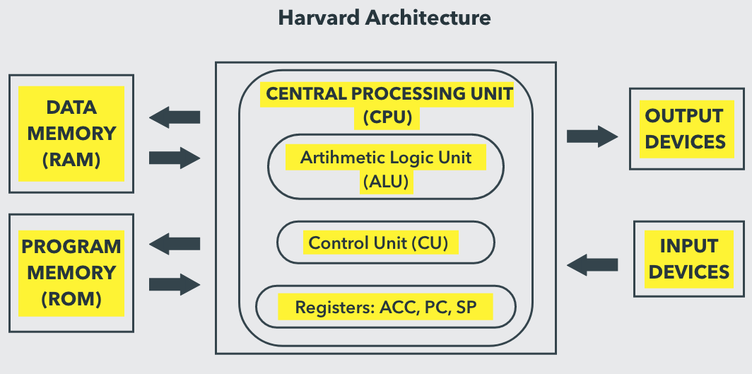
Harvard Architecture
In contrast to Von Neumann architecture, Harvard architecture uses separate memory for Instruction (Program) and Data. The Harvard Architecture’s separate Instruction Memory and Data Memory also have independent signal pathways or buses, so the CPU can access both Instructions and Data at the same time.
Harvard Architecture is used by almost all microcontrollers, including the 8051.
.
8051 Microcontroller Memory Organization
Program Memory (ROM) and Data Memory are independent components of the 8051 microcontroller memory (RAM). The program to be executed, or the instructions, are stored in the program memory of the 8051 microcontrollers. On the other hand, temporary variable data and interim findings are kept in the data memory.
Internal ROM and Internal RAM are both features of the 8051 Microcontroller. If the internal memory is insufficient, you can use the right circuits to add external memory.
Program Memory (ROM) of 8051 Microcontroller
The program memory, commonly known as the ROM of the microcontroller, houses the code or instructions that must be carried out by the 8051 microcontrollers. 4KB of inbuilt ROM are present in the original Intel 8051 Microcontroller.
The 8031 and 8032 series of 8051 variations, for example, lack internal ROM (Program Memory) and must be interfaced with external Program Memory that has instructions loaded in it.
Nearly all contemporary 8051 microcontrollers, including the 8052 Series, include 8KB of internal flash memory that can be reprogrammed.
The address range for internal ROM with 4KB is 0000H to 0FFFH. When this threshold is reached, the CPU will automatically fetch the code from the external program memory if the address space, or program addresses, exceeds it.
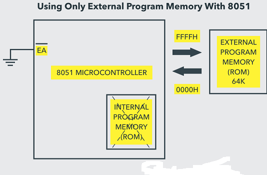
When the External Access Pin (EA Pin) is HIGH, the CPU first retrieves instructions from the Internal Program Memory in the address range of 0000H to 0FFFFH, and if the memory addresses exceed the limit, then the instructions are retrieved from the external ROM in the address range of 1000H to FFFFH.

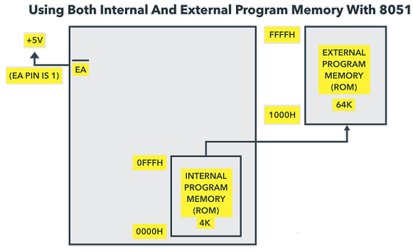
Another method of retrieving the instructions is to completely disregard the Internal ROM and retrieve every instruction from the External Program Memory instead (External ROM). The EA Pin must be linked to GND in this case. The external ROM’s memory locations in this scenario range from 0000H to FFFFH.
Data Memory (RAM) of 8051 Microcontroller
Temporary information and interim outcomes produced and used throughout the 8051 microcontroller’s typical operation are stored in the data memory, or RAM, of the device. The internal RAM of the original Intel 8051 microcontroller was 128 KB.
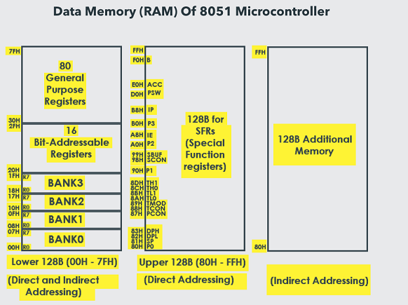
However, 256B of RAM is present in practically all contemporary 8051 Microcontroller variations. This 256B is divided into Working Registers (arranged as Register Banks), Bit-Addressable Area, and General Purpose RAM for the first 128B of the 256B. (also known as the Scratchpad area).
The first 32B, or memory from addresses 00H to 1FH, of the first 128B of RAM (from 00H to 7FH), is made up of 32 Working Registers that are arranged in four banks with eight Registers in each bank.
The correct Bank must first be chosen in order to address the register by name. The RS0 and RS1 bits of the Program Status Word (PSW) Register must be used to choose the bank (RS0 and RS1 are the 3rd and 4th bits in the PSW Register).

Bank0, Bank1, Bank2, and Bank3 are the names of the four banks. R0 through R7 are the 8 registers that make up each bank. There are two methods to address each Register: either by name or by address.
To address the register by name, first, the corresponding Bank must be selected. In order to select the bank, we have to use the RS0 and RS1 bits of the Program Status Word (PSW) Register (RS0 and RS1 are the 3rd and 4th bits in the PSW Register).
The appropriate Bank may or may not be chosen when addressing the Register using its address, for example, 12H. (12H) is equivalent to R2 in Bank2.
From 20H to 2FH, the following 16B of the RAM, are Bit-Addressable memory regions. There are a total of 128 bits, each of which can be addressed using the digits 00H to 7FH, or the complete byte using the digits 20H to 2FH.
For instance, bit 2 of internal RAM address 26H is 32H.
The general purpose RAM section, which is byte addressable, is located in the final 80B of the internal RAM, or at addresses from 30H to 7FH.
You can directly or indirectly address the lower 128B of RAM.
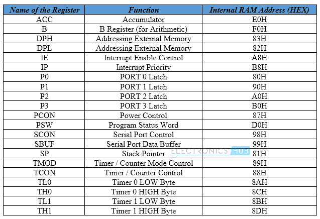
Memory locations from 80H to FFH, or the upper 128B of the RAM, are reserved for Special Function Registers (SFRs). Specific 8051 Microcontroller functionalities are controlled via SFRs. I/O Port Registers (P0, P1, P2, and P3), PSW (Program Status Word), A (Accumulator), IE (Interrupt Enable), PCON (Power Control), and other SFRs are a few examples of SFRs.
Memory addresses in SRFs can only be accessed directly. The addresses between 80H and FFH cannot be used as additional RAM space even though some of them have no SFR assigned to them.
There may be an additional 128B of RAM in some microcontrollers, which shares the memory address (80H to FFH) with SFRs. However, the only way to reach this extra RAM block is through indirect addressing.
Interfacing External Memory with 8051 Microcontroller
Having the opportunity to increase a microcontroller’s capabilities, whether they pertain to memory, input/output (IO), or anything else, is always a good thing. This growth will be helpful to prevent design throttling. A common 8051 microcontroller contains 4KB of ROM and 128B of RAM, as we’ve seen (most modern 8051 Microcontroller variants have 8K ROM and 256B of RAM).
The internal RAM and ROM of an 8051 Microcontroller-based system are not the only resources available to the system designer. Both external RAM and ROM, or data memory and program memory, can be connected.
Due to the fact that complicated programs written in high-level languages frequently get larger and take up more memory, external program memory, also known as ROM, is typically interfaced.
Another significant factor is the requirement to interact with external ROM for processors like 8031 or 8032, which lack internal ROM.
Program memory (ROM) and data memory (RAM) can each have a maximum interface size of 64KB with the 8051 microcontrollers.
The block diagram for connecting the 8051 microcontrollers to 64KB of external RAM and 64KB of external ROM is shown in the accompanying figure.
It’s crucial to keep in mind that Port 0 (P0) cannot be utilized as an IO port because it will be used for a multiplexed address and data bus when connecting external memory to an 8051 microcontroller (A0 – A7 and D0 – D7). Port 2 might be utilized as the higher byte of the address bus, though not necessarily.
Conclusion
I hope all of you understand the basics of 8051 Microcontroller Memory Organization, Program Memory, Data Memory, Internal ROM, and RAM and how to interface external Memory (ROM and RAM) with 8051 Microcontroller. We MATHA ELECTRONICS will be back soon with more informative blogs.