
I am text block. Click edit button to change this text. Lorem ipsum dolor sit amet, consectetur adipiscing elit. Ut elit tellus, luctus nec ullamcorper mattis, pulvinar dapibus leo.
-25%

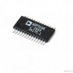
ADP3168 6-Bit, Programmable 2-, 3-, 4-Phase Synchronous Buck Controller IC
Original price was: ₹65.00.₹55.00Current price is: ₹55.00. inc. GST
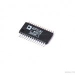
ADP3180 6-Bit Programmable 2-, 3-, 4-Phase Synchronous Buck Controller IC
Original price was: ₹65.00.₹55.00Current price is: ₹55.00. inc. GST
74HC74 Dual D-Type Flip-Flop with Set and Reset; Positive Edge-Trigger
Original price was: ₹20.00.₹15.00Current price is: ₹15.00. inc. GST
- Dual D-type flip-flop with set and reset; positive edge-trigger
- Number of Circuits: 2
- Logic Family: 74HC
- Input Type: Single-Ended
- Output Type: Differential
- Propagation: Delay Time: 44 ns
- Output Current: 5.2mA
- No. of Pins: 14
- Operating Temperature Range: -40°C to +85°C
- Supply Voltage Range: 2V to 6V
- Package: DIP14
Description
The 74HC74 designed as a dual positive edge-triggered D-type flip-flop. The 74HC74 consists of dual positive-edge triggered, D-type flip-flops with individual data (D) inputs, clock (CP) inputs, set (SD) and reset (RD) inputs; also complementary Q and Q outputs. The Data at the D-input, that meets the set-up and hold time requirements on the LOW-to-HIGH clock transition, stored in the flip-flop and appears at the Q output. Schmitt-trigger function in the clock input, makes the circuit highly tolerant to slower clock rise and fall times. Whereas the Inputs include clamp diodes that enable the use of current limiting resistors to interface inputs to voltages in excess of VCC.
The 74HC/HCT74 is a high-speed Si-gate CMOS device and is pin compatible with low power Schottky TTL
(LSTTL). They are specified in compliance with JEDEC standard no. 7A. The D flip-flop is an edge triggered device which transfers input data to Q on clock rising or falling edge. Data Latches are level sensitive devices such as the data latch and the transparent latch.
The 74HC74 (7474) integrated circuit provides two independent D-type flip flops in a single package. The flip flop triggered on the positive edge of a clock pulse. At the moment the clock pin (CLK) goes high, the state of data pin (D)captured and held as output (Q). Q will not change again until the next time the clock rises, regardless of how long the clock stays high, or any further changes to D.
Reviews (0)
Shipping & Delivery

Related products


1/4W 5% Assorted Value Carbon Film Resistor Assortment Kit Set pack electronic diy kit
- 100% brand new and high quality.
- Fine workmanship and long service life.
- 1/4W carbon film resistor package.
- High precision and stability.
- Easy to use.
- Precision: 5%
- Error: 5%
- Values
- 10Ω, 15Ω, 22Ω, 33Ω, 47Ω, 68Ω, 100Ω, 220Ω, 330Ω, 470Ω, 1k, 1k5, 2k2, 3k3, 4k7, 5k6, 6K8, 8K2, 10K, 15K, 22K, 33K, 47K, 56K, 68K, 100K, 150K, 220K, 330K, 470K
- Package included: 150pcs

25pcs Button Switch Kit
- Relative Humidity: 95%
- Rated Voltage: 12V
- Rated Current: 50 mA
- Contact resistance: 50M Ohm Max (initial)
- The insulation resistance: 100M Ohm minDC (250V)
- The compressive strength: AC250V (50/60Hz for 1 minute)
- Mechanical life: 100000 cycles
- The environment temperature: 25° ~ + 105°
- The operating strength: 180/250 (plus or minus 30gf)
- Dimension: 12 * 12 * 7.3 round convex type
- Total Buttons: 25pcs
- Colours: 5 (Black, Red, White, Blue, Yellow)


650NM Laser Diode
- Wavelength: 650nm
- Output optical power: 5mW
- Operating voltage: 5V
- Operating current: ~30mA
- Input current: 30mA
- Housing material: Copper
- Power lead length: 120mm.
- Transmit power: 58mW
- Spot: size 10mm to 15mm at 15meters
- Life span more than 2000 hours
- Driver circuit: APC circuit
- Small size
- Cost-effective
- Breadboard friendly
- Operating temperature -10°C to 40°C
- Dimension: :15mm x 6mm
- Weight: 10 grams


ADXL 335 Accelerometer IC
- 3-axis sensing
- Small, low profile package
- 4 mm × 4 mm × 1.45 mm LFCSP
- Low power : 350 μA (typical)
- Single-supply operation: 1.8 V to 3.6 V
- 10,000 g shock survival
- Excellent temperature stability
- BW adjustment with a single capacitor per axis
- RoHS/WEEE lead-free compliant
- 8V- 3.6V single-supply operation
- Integrated X, Y, and Z axis accelerometer on a single chip
- X and Y axis has a 0.5Hz to 1600Hz bandwidth
- Z axis has a 0.5Hz to 550Hz bandwidth
- Hermetically sealed for temp and humidity resistance
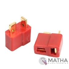
Dean Connector
- Male plug size: About 13* 7* 19mm
- Female plug size: About 13* 7* 15mm
- Current Rating: 30Amps
- Colour: Red and golden
- Material: Plastic and metal
- Provides a secure connection for battery and motor connections
- Eliminates the possibility of wrong polarity connections
- Used in RC hobby, car, boat, plane, helicopter, LIPO battery, etc.
- Dimension: 9x0.7x2cm
- Weight:20gm
Reviews
There are no reviews yet.