
I am text block. Click edit button to change this text. Lorem ipsum dolor sit amet, consectetur adipiscing elit. Ut elit tellus, luctus nec ullamcorper mattis, pulvinar dapibus leo.
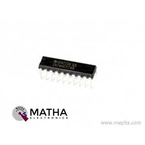
74LS374 Edge-Triggered D Flip-Flop IC
Original price was: ₹23.00.₹18.00Current price is: ₹18.00. inc. GST
CD4099 8-Bit Addressable Latch IC
Original price was: ₹30.00.₹25.00Current price is: ₹25.00. inc. GST
74LS574 Octal Edge Triggered D Flip-Flop IC
- Octal Edge Triggered D Flip-Flop With 3-State Output
- High-level input voltage: 1.5V
- Low-level input voltage: 0.5V
- Input clamp current: ±20mA
- Maximum clock frequency: 5MHz
- Propagation delay time: 265ns
- Supply voltage range: 2 to 6V
- Package: DIP-20
Description
The 74LS574 comes as a part of the 74XXYY IC series. The 74LS574 designed as a high-speed, low-power Octal D-type Flip-Flop featuring separate D-type inputs for every flip-flop. And 3-state outputs for bus-oriented applications. The two sections of the IC controlled independently by the buffered Clock (CP) and Output Enable (OE) control gates provided to all flip-flops in the IC.
The register is fully edge-triggered. The data presented to the D inputs stored within the flip-flops on the LOW-to-HIGH Clock (CP) transition. The state of every D input, one setup time before the Low-to-High clock transitiontransferred to the corresponding flip-flop’s Q output. The 3-State output buffers drive heavily loaded 3-State buses, MOS memories, or MOS microprocessors. Moreover, the active Low Output Enable (OE) controls all eight 3-State buffers independently of the latch operation. Under the condition, when OE is Low, the latched or transparent data appears at the outputs. When OE is High, the outputs are during a high impedance “off” state, which suggests they’re going to neither drive nor load the bus.
A D-type latch/flip-flop with two stable states that is designed as a timed latch. A D-type latch has a one-clock-cycle delay in its input. Delay circuits are frequently produced by cascading multiple D-type flip-flops. This was then used in a variety of applications, such as digital television systems. A D flip-flop, sometimes known as a delay flip-flop, is a D-type flip-flop.
Applications
- Function as a digital building block for a wide variety of temporary data storage & processing devices such as SRAMs & DRAMs etc.
- Also Useful as Input or Output Port for Microprocessors
Reviews (0)
Shipping & Delivery

Related products


5-36v Switch Drive High-power MOSFET Trigger Module
- Operating Voltage: DC 5V - 36V;
- The trigger source: digital high-low (DC3.3V - 20V), can be connected microcontroller IO port, PLC interfaces, DC power, you can access the PWM signal, the signal frequency 0--20KHZ perfect support.
- Output capacity: DC 5V - 36V, at room temperature, continuous current 15A, power 400W! Lower auxiliary cooling conditions, the maximum current up to 30A.
- Applications: You can control the output of power equipment, motors, light bulbs, LED lights, DC motors, micro-pumps, solenoid valves, etc.. You can enter
- PWM, motor speed control, lamp brightness.
- Availability: unlimited switch
- Operating temperature: -40-85
- Dimension: 34mm x 17mm x 12mm
- The use of imported dual-MOS parallel active output, lower resistance, more current, strong power at room temperature, 15A, 400W, to meet the most use of the equipment
- Wide voltage, the perfect support for PWM
- Easily control high power devices
- Input PWM to achieve motor speed control, lamp brightness control

ADXL 335 Accelerometer IC
- 3-axis sensing
- Small, low profile package
- 4 mm × 4 mm × 1.45 mm LFCSP
- Low power : 350 μA (typical)
- Single-supply operation: 1.8 V to 3.6 V
- 10,000 g shock survival
- Excellent temperature stability
- BW adjustment with a single capacitor per axis
- RoHS/WEEE lead-free compliant
- 8V- 3.6V single-supply operation
- Integrated X, Y, and Z axis accelerometer on a single chip
- X and Y axis has a 0.5Hz to 1600Hz bandwidth
- Z axis has a 0.5Hz to 550Hz bandwidth
- Hermetically sealed for temp and humidity resistance
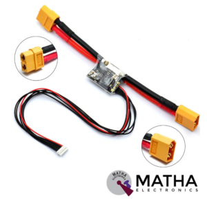
APM/Pixhawk Power Module V6.0 Output BEC 3A XT60 Plug 28V 90A
- Input Voltage Range: 6-28V DC
- Output voltage: 5.3V ± 0.1V
- Maximum output current: 3A
- Maximum current: 90A
- Maximum voltage: 30V
- Supports from 2 cell to 6 cell battery.
- 6P cable can be directly connected to APM/Pixhawk flight control
- Additional 4P rows of pin-free to wire/PIN to connect to another flight control
- Voltage and current measurement configured for 5V ADC.
- Switching regulator outputs 5.3V and 3A max.
- Dimensions: 25mm x 21mm x 9mm
- Weight: 17gm


Dual Micro USB 3.7v to 5V 2A Power Bank DIY 18650 LiPo Charger
- 4-level LED lamp display power, not working state intelligent automatic shutdown;
- The built-in lithium battery protection IC, over-current, under-voltage protection;
- Dual USB output ports.
- Dimensions: 68 x 34 x 9 mm (LxWxH)
- Weight: 10 gm
- Input port: MicroUSB (Andro)
- Input requirements: 5V constant voltage power supply can do charge input power, the most matching charger for 5v1a above
- Output port: USB
- Output parameters: 5V1A/5V2A
- Requirements for rechargeable batteries:
- Compatible Batteries: 18650 batteries, cell phone batteries, flat-panel batteries, MP3 batteries, etc. 3.7v-4.2V polymer Lithium battery,
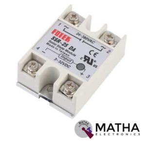
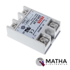
Solid State Relay Module SSR-25DA 25A /250V 3-32V DC Input 24-380VAC Output
- Control mode: DC-AC
- Input voltage: 3-32V DC.
- Output voltage: 24-380V AC.
- Output current: 25A.
- Working voltage: 250V.
- Material: plastic + metal.
- Environment temperature: -30 to +75
- Long service life and high reliability.
- Reduced electromagnetic interference.
- Highly reliable, compact size designed to offer users maximum simplicity.
- Dimension: 6. 5Cm x 4. 5Cm x 2. 2Cm


TP5100 4.2v 8.4v Single Double Lithium Battery Charge Management Li-ion Battery Compatible 2A Charging Board
- Input voltage: 5-15V DC power supply.
- Charge status: full and unloaded blue lights, charging red.
- Double 8.4v / 4.2v lithium rechargeable single .
- Programmable charge current. 0. 1A-2A .
- Programmable steady precharge current 10% -100%.
- Wide operating voltage, maximum reach I8V.
- Red and green LED charge status indicator.
- Chip temperature protection, overcurrent protection, under voltage protection.
- Battery temperature protection, reverse battery shutdown, short circuit protection.
- Switching frequency 400Khz, usable inductance 20uH and more.
- PWR_ON Power battery for switching control.
Reviews
There are no reviews yet.