
I am text block. Click edit button to change this text. Lorem ipsum dolor sit amet, consectetur adipiscing elit. Ut elit tellus, luctus nec ullamcorper mattis, pulvinar dapibus leo.
-5%

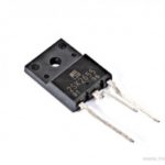
2SK2655 N-Channel Mosfet Transistor 900V 8A
Original price was: ₹200.00.₹150.00Current price is: ₹150.00. inc. GST
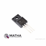
2SK2645 N-Channel Mosfet Transistor 600V 9A
Original price was: ₹95.00.₹85.00Current price is: ₹85.00. inc. GST
74LS76 Dual J-K Flip-Flop IC with Set and Clear
Original price was: ₹210.00.₹200.00Current price is: ₹200.00. inc. GST
- Dual JK Flip-Flop With Set and Clear
- Maximum Clock Frequency: 45MHz
- High-level input voltage: 2V
- Low-level input voltage: 0.8V
- High-level output current: -0.4mA
- Low-level output current: 8mA
- No. of Circuits: 2
- Input clamp voltage: -1.5V
- Supply voltage range: 4.5 to 5.5V
- Package: DIP-16
Description
The 74LS76 designed with separate J, K, clock pulse, direct clear inputs, and direct set. These flip-flops are developed in such how when the clock is set HIGH, data are going to be received enabling inputs. This IC consists of two JK flip-flops where each flip-flop is utilized individually for the specified applications. These flip-flops are widely utilized in control registers, shift registers, and storage registers, And are referred to as latching devices thanks to their ability to recollect every single bit of data. These devices latch the output supported by the stored binary data. It’s important to notice over one flip-flop are often combined serial for storing a little amount of data as an EEPROM. Moreover, the 74LS76 operates at a voltage range of 2V to 6V and is made in 14-pin PDIP, GDIP, PDSO packages.
This JK flip-flop is the perfect tool for practical applications because it possesses stable output for all kinds of inputs. The J and K inputs logic levels function as per the reality Table as long as minimum set-up times are taken into observation. Meanwhile, the input data is transferred to the outputs when the HIGH-to-LOW clock transition occurs.
With the addition of the clock input circuitry, the JK Flip Flop was developed as a gated RS flip flop. The invalid state occurs when both the S and R inputs are capable of logic “1.” A clock circuit is introduced to prevent this invalid state. Due to the addition of the timed input, the JK Flip Flop now has four possible input combinations. “Logic 1”, “logic 0”, and “logic 1” are the four inputs. “No change” and “Toggle” are two options.
APPLICATION
- Employed in Memory/Control Registers
- Used in Shift Registers
- Used in Latching devices
- Incorporated in EEPROM circuits
Reviews (0)
Shipping & Delivery

Related products


ADXL 335 Accelerometer IC
- 3-axis sensing
- Small, low profile package
- 4 mm × 4 mm × 1.45 mm LFCSP
- Low power : 350 μA (typical)
- Single-supply operation: 1.8 V to 3.6 V
- 10,000 g shock survival
- Excellent temperature stability
- BW adjustment with a single capacitor per axis
- RoHS/WEEE lead-free compliant
- 8V- 3.6V single-supply operation
- Integrated X, Y, and Z axis accelerometer on a single chip
- X and Y axis has a 0.5Hz to 1600Hz bandwidth
- Z axis has a 0.5Hz to 550Hz bandwidth
- Hermetically sealed for temp and humidity resistance
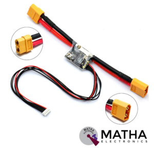
APM/Pixhawk Power Module V6.0 Output BEC 3A XT60 Plug 28V 90A
- Input Voltage Range: 6-28V DC
- Output voltage: 5.3V ± 0.1V
- Maximum output current: 3A
- Maximum current: 90A
- Maximum voltage: 30V
- Supports from 2 cell to 6 cell battery.
- 6P cable can be directly connected to APM/Pixhawk flight control
- Additional 4P rows of pin-free to wire/PIN to connect to another flight control
- Voltage and current measurement configured for 5V ADC.
- Switching regulator outputs 5.3V and 3A max.
- Dimensions: 25mm x 21mm x 9mm
- Weight: 17gm


Dual Micro USB 3.7v to 5V 2A Power Bank DIY 18650 LiPo Charger
- 4-level LED lamp display power, not working state intelligent automatic shutdown;
- The built-in lithium battery protection IC, over-current, under-voltage protection;
- Dual USB output ports.
- Dimensions: 68 x 34 x 9 mm (LxWxH)
- Weight: 10 gm
- Input port: MicroUSB (Andro)
- Input requirements: 5V constant voltage power supply can do charge input power, the most matching charger for 5v1a above
- Output port: USB
- Output parameters: 5V1A/5V2A
- Requirements for rechargeable batteries:
- Compatible Batteries: 18650 batteries, cell phone batteries, flat-panel batteries, MP3 batteries, etc. 3.7v-4.2V polymer Lithium battery,
GSM Antenna Dlenp 2dbi/3dbi Patch Antenna with SMA Male Connector
- GSM Antenna
- Gain: 2 to 3dbi
- Wire Length: 3 metre
- 3dbi Sticker Antenna
- GSM Antenna
- SMA Male Connector
- Frequency Range(MHz): 824-960/1710-1990Mhz
- Bandwidth (MHz): 136/280
- VSWR≤1.5
- Gain(dB): 2-3dbi
- Max Input power(W): 60W
- Input Impedance: 50 Ω
- Polarization Type: Vertical
- Cable Type: RG174
- Mounting Adhesive
- Net weight: 47g


TP5100 4.2v 8.4v Single Double Lithium Battery Charge Management Li-ion Battery Compatible 2A Charging Board
- Input voltage: 5-15V DC power supply.
- Charge status: full and unloaded blue lights, charging red.
- Double 8.4v / 4.2v lithium rechargeable single .
- Programmable charge current. 0. 1A-2A .
- Programmable steady precharge current 10% -100%.
- Wide operating voltage, maximum reach I8V.
- Red and green LED charge status indicator.
- Chip temperature protection, overcurrent protection, under voltage protection.
- Battery temperature protection, reverse battery shutdown, short circuit protection.
- Switching frequency 400Khz, usable inductance 20uH and more.
- PWR_ON Power battery for switching control.
Reviews
There are no reviews yet.