
I am text block. Click edit button to change this text. Lorem ipsum dolor sit amet, consectetur adipiscing elit. Ut elit tellus, luctus nec ullamcorper mattis, pulvinar dapibus leo.
-17%
")
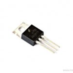
7815 15V Positive Voltage Regulator IC
Original price was: ₹18.00.₹15.00Current price is: ₹15.00. inc. GST
75188 Quadruple Line Driver IC
Original price was: ₹35.00.₹30.00Current price is: ₹30.00. inc. GST
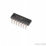
CD4010 Hex Buffer Converter IC
Original price was: ₹24.00.₹20.00Current price is: ₹20.00. inc. GST
- Hex Buffer/Converter
- Input Current: ±10mA
- Power Dissipation: 300mW
- High level Output Voltage: 5.0V
- Low level Output Voltage Max.: 0.05V
- High level Input Voltage: 2.75V
- Low level Input Voltage: 2.25V
- Low level Output Current: 7mA
- High level Output Current: -1.2mA
- Propagation Delay Time Max.: 200ns
- Package: DIP-16
Description
CD4010 made up of monolithic complementary MOS (CMOS) technology, integrated with p-type and n-type enhancement mode transistors. As a result, the output swings are practically equal to the supply voltage, resulting in a symmetrical circuit. The IC also has buffered outputs with very high gain, which improves transfer characteristics. All of the inputs of this IC are protected from static discharge by diodes connected to VDD and VSS. During static circumstances, no DC power is consumed other than that generated by leakage current. VCC VDD is provided through conversion ranges of 3V to 15V. The devices also feature buffered outputs, which provide very high gain and improve transfer characteristics.
The IC can function in a variety of environments and at a variety of operating voltages, and it can directly link with other hex buffers, CMOS to DTL or TTL interfaces, or as CMOS current drivers. CD4010 also has excellent noise immunity and ESD protection. They have equal source and sink current capacities and follow the B series output drive standard. The CD4010 IC is available in 16-pin dual in line package (DIP)ceramic (D) packages that are hermetically sealed. And it works with a voltage range of 3 to 15 volts.
CMOS to TTL or DTL logic-level converters or CMOS high-sink-current drivers can be utilised with the CD4010B hex buffer/converter. In all applications except multiplexers, the CD4050B is the recommended hex buffer replacement for the CD4010B. The CD4069UB hex inverter is ideal for situations that do not require a lot of sink current or voltage conversion. The CD4010B is available in hermetic dual-in-line ceramic (D) packaging with 16 leads.
APPLICATIONS
- CMOS to DTL/TTL Hex Converter
- Multiplexer: 1-to-6 or 6-to-1
- CMOS Current “Sink” or “Source” Driver
- CMOS High-to-Low Logic-Level Converter
Reviews (0)
Shipping & Delivery

Related products


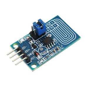
Capacitor Touch Dimmer, Constant Voltage LED Stepless Dimming, PWM Control Board
- Voltage range: 4V to 5V
- Maximum output current: 500mA
- Hole distance: 16 mm
- Aperture: 5 mm
- The lamp brightness can be adjusted by requirement, it is very to operate.
- It can touch in medium protection, such as glass, acrylic, plastic, ceramics, and so on, which is very safe.
- Anti power and phone interference, the EFT can reach above +/-2KV; the touch response sensitivity and reliability will not be affected by the close distance or multi-angle mobile phone interference.
- Dimming mode: Non-polar PWM dimming.
- PCB size: 23 x 20mm

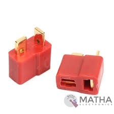
Dean Connector
- Male plug size: About 13* 7* 19mm
- Female plug size: About 13* 7* 15mm
- Current Rating: 30Amps
- Colour: Red and golden
- Material: Plastic and metal
- Provides a secure connection for battery and motor connections
- Eliminates the possibility of wrong polarity connections
- Used in RC hobby, car, boat, plane, helicopter, LIPO battery, etc.
- Dimension: 9x0.7x2cm
- Weight:20gm
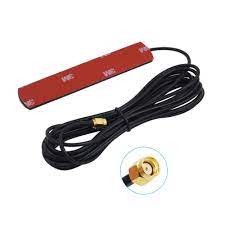
GSM Antenna Dlenp 2dbi/3dbi Patch Antenna with SMA Male Connector
- GSM Antenna
- Gain: 2 to 3dbi
- Wire Length: 3 metre
- 3dbi Sticker Antenna
- GSM Antenna
- SMA Male Connector
- Frequency Range(MHz): 824-960/1710-1990Mhz
- Bandwidth (MHz): 136/280
- VSWR≤1.5
- Gain(dB): 2-3dbi
- Max Input power(W): 60W
- Input Impedance: 50 Ω
- Polarization Type: Vertical
- Cable Type: RG174
- Mounting Adhesive
- Net weight: 47g
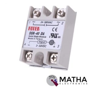

Solid State Relay SSR-40DD 40A 3-32V DC to 5-60V DC SSR 40DD Relay Solid State
- Model: SSR-40 DD.
- Control mode: DC-DC
- Input voltage: 3-32V DC.
- Output voltage: 5-60V DC.
- Output current: 40A.
- On voltage: ≤1v.
- One-off time: ≤10ms.
- Off leakage current: ≤2ma.
- Loading current: 40A
- Control current: 3-25mA DC
- Material: plastic + metal.
- Environment temperature: -30 to +75
- Long service life and high reliability.
- Reduced electromagnetic interference.
- Highly reliable, compact size designed to offer users maximum simplicity.
- Weight: 0. 106Kg.
Reviews
There are no reviews yet.