
I am text block. Click edit button to change this text. Lorem ipsum dolor sit amet, consectetur adipiscing elit. Ut elit tellus, luctus nec ullamcorper mattis, pulvinar dapibus leo.
-22%
D3SB60 Flat Bridge Rectifier 3A 600V
Original price was: ₹26.00.₹20.00Current price is: ₹20.00. inc. GST
70N10 N-Channel Power Mosfet Transistor 100V 65A
Original price was: ₹160.00.₹135.00Current price is: ₹135.00. inc. GST
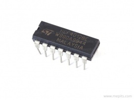
CD4012 Dual 4 Input NAND Gate IC
Original price was: ₹23.00.₹18.00Current price is: ₹18.00. inc. GST
- Dual 4 Input NAND Gate:
- Logic Family: HCF40
- No Of Gates: 2
- No Of Input Lines: 4
- No Of Output Lines: 1
- Supply Voltage Range: 3 to 20V
- Input Current: ±10mA
- High Level Output Current: – 2.4 mA
- Low Level Output Current: 2.4 mA
- Low level Output Voltage: 0.05V
- High level Output Voltage Min.: 4.95V
- Low level Input Voltage Max.: 1.5V
- High level Input Voltage Min.: 3.5V
- Power Dissipation: 200mW
- Operating Temperature: -55 to +1250C
- Propagation Delay Time Max.: 250ns
- Package: DIP-14
Description
CD4012 belongs to the CD4000 IC series. This CD4012 designed as a monolithic 4-input NAND gate IC designed by implementing the complementary MOS technology, integrated with P and N-type enhancement mode transistors. As a result, provide a symmetrical circuit with output swings essentially equal to the supply voltage. CD4012 manufactured in a 14-lead dual-in-line plastic or ceramic package and plastic micro package. The CD4012 IC operates at a wide range of working voltage, a wide range of working conditions. And directly interfaces with CMOS, NMOS, and TTL. The output of the IC always comes in TTL which makes it quite easy to function with other TTL devices and microcontrollers.
Moreover, CD4012 features ESD barring and high noise immunity. Each output is protected against static damage by using clamping diodes. CD4012 Operates at a supply voltage of range between 3V to 20V. This IC is designed for operation over the full military temperature range of 0°C to 70°C. CD4012 Dual 4 Input NAND Gate IC feature a Propagation Delay Time of Max 250ns and Power Dissipation of 250mW.
NAND gate defined as a digital logic gate most commonly used in DLD applications. It nalso sometimes referred to as a universal logic gate, and used to implement any logic gate or expression in existence. In case, if any one of the inputs to the NAND gate switch to high, the output of the gate will always be a logical low. On the other hand, a NAND gate yields a logical high only when all of its inputs set to LOW.
Application
- Automotive
- Alarm system
- Data terminals
- Industrial controls
- Instrumentation
- Remote metering
- Medical Electronics
- Computers
Reviews (0)
Shipping & Delivery

Related products


1/4W 5% Assorted Value Carbon Film Resistor Assortment Kit Set pack electronic diy kit
- 100% brand new and high quality.
- Fine workmanship and long service life.
- 1/4W carbon film resistor package.
- High precision and stability.
- Easy to use.
- Precision: 5%
- Error: 5%
- Values
- 10Ω, 15Ω, 22Ω, 33Ω, 47Ω, 68Ω, 100Ω, 220Ω, 330Ω, 470Ω, 1k, 1k5, 2k2, 3k3, 4k7, 5k6, 6K8, 8K2, 10K, 15K, 22K, 33K, 47K, 56K, 68K, 100K, 150K, 220K, 330K, 470K
- Package included: 150pcs


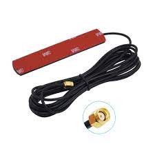
GSM Antenna Dlenp 2dbi/3dbi Patch Antenna with SMA Male Connector
- GSM Antenna
- Gain: 2 to 3dbi
- Wire Length: 3 metre
- 3dbi Sticker Antenna
- GSM Antenna
- SMA Male Connector
- Frequency Range(MHz): 824-960/1710-1990Mhz
- Bandwidth (MHz): 136/280
- VSWR≤1.5
- Gain(dB): 2-3dbi
- Max Input power(W): 60W
- Input Impedance: 50 Ω
- Polarization Type: Vertical
- Cable Type: RG174
- Mounting Adhesive
- Net weight: 47g


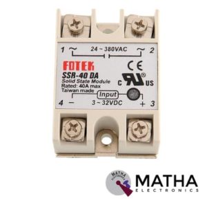
Solid State Relay Module DC To AC SSR-40DA 3-32VDC/24-380VAC 40A
- Control mode: DC-AC
- Input voltage: 3-32V DC.
- Output voltage: 24-380V AC.
- Output current: 40A.
- Working voltage: 250V.
- Material: plastic + metal.
- Loading current: 40A
- Control current: 3-25mA DC
- On voltage: ≤1.5V AC
- One-off Time: ≤10ms
- Off Leakage Current: ≤2mA
- Dielectrics voltage-resistance: 2500VAC
- Environment temperature: -30 to +75
- Long service life and high reliability.
- Reduced electromagnetic interference.
- Highly reliable, compact size designed to offer users maximum simplicity.


TP5100 4.2v 8.4v Single Double Lithium Battery Charge Management Li-ion Battery Compatible 2A Charging Board
- Input voltage: 5-15V DC power supply.
- Charge status: full and unloaded blue lights, charging red.
- Double 8.4v / 4.2v lithium rechargeable single .
- Programmable charge current. 0. 1A-2A .
- Programmable steady precharge current 10% -100%.
- Wide operating voltage, maximum reach I8V.
- Red and green LED charge status indicator.
- Chip temperature protection, overcurrent protection, under voltage protection.
- Battery temperature protection, reverse battery shutdown, short circuit protection.
- Switching frequency 400Khz, usable inductance 20uH and more.
- PWR_ON Power battery for switching control.
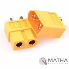
XT60 Connector
- Manufacturer: AMASS
- Connector Series: XT60H
- Rated Voltage: DC 500V
- Metal Material: Brass Gold Plated
- Rated Current: 30A
- Momentary Current: 60A
- Number of pins: 2
- Colour: Yellow
- Contact Resistance: 0.55mΩ
- FR Level: UL94 V0
- Use Times: 1000 TIMES
- Temperature: -20℃ to 120℃
- Spatial Orientation Straight
- Compatible for Wire size up to 12AWG
- Mechanical mounting for cable
- Electrical mounting soldered
- Contact plating Gold flash
Reviews
There are no reviews yet.