
I am text block. Click edit button to change this text. Lorem ipsum dolor sit amet, consectetur adipiscing elit. Ut elit tellus, luctus nec ullamcorper mattis, pulvinar dapibus leo.
-33%

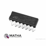
CD4013 Dual D-type Flip-Flop IC
Original price was: ₹33.00.₹25.00Current price is: ₹25.00. inc. GST
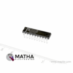
74LS373 Octal D-Type Transparent Latch IC
Original price was: ₹25.00.₹15.00Current price is: ₹15.00. inc. GST
CD4027 Dual J-K Master Slave Flip-Flop IC
Original price was: ₹30.00.₹20.00Current price is: ₹20.00. inc. GST
- Dual J K Master Slave Flip Flop
- Supply Voltage Range: 3 to 15V
- Input Current: ±10mA
- Power Dissipation: 200mW
- Low level Output Voltage Max.: 0.05V
- High level Output Voltage Min.: 4.95V
- Low level Input Voltage Max.: 1.5V
- High level Input Voltage Min.: 3.5V
- Propagation Delay Time Max.: 300ns
- Maximum Clock Frequency: 24MHz
- Package: DIP-16
Description
CD4027 Dual J-K Master-Slave Flip-Flop IC belongs to the CD4XXX IC series. The IC is constructed by using the monolithic complementary MOS (CMOS), integrated with p-type and n-type enhancement mode transistors. Each flip-flop comprises of independent J, K, set, reset, and clock inputs and buffered Q and Q outputs. These flip-flops comes as a edge sensitive to the clock input and change state on the positive-going transition of the clock pulses. Moreover, the Set or reset pin on the IC is independent of the clock and accomplished by a high level on the respective input. The output of the IC always comes in TTL. And is easily interfaced with other TTL, CMOS, and NMOS devices. The IC provides wide range of features such as high noise immunity and low thermal dissipation. And also all inputs are protected against damage because of static discharge by diode clamps to VDD and VSS.
CD4027 designed as a single monolithic chip microcircuit comprised of two identical complementary-symmetry J-K master-slave flip-flops. Moreover, each flip-flop offers arrangements for individual J, K, Set Reset, and Clock input signals. And also the Buffered Q and Q signals are provided as outputs.
The JK Flip Flop designed as a gated RS flip flop with the addition of the clock input circuitry. When both the inputs S and R are capable logic “1”, the invalid condition takes place. Inorder to prevent this invalid condition, a clock circuit is introduced. The JK Flip Flop consists of four possible input combinations because of the addition of the clocked input. The four inputs are “logic 1”, ‘logic 0”. “No change’ and “Toggle”.
Application
- Shift Registers
- Ripple Binary Counters
Reviews (0)
Shipping & Delivery

Related products


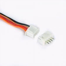


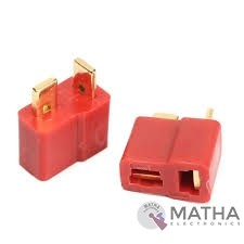
Dean Connector
- Male plug size: About 13* 7* 19mm
- Female plug size: About 13* 7* 15mm
- Current Rating: 30Amps
- Colour: Red and golden
- Material: Plastic and metal
- Provides a secure connection for battery and motor connections
- Eliminates the possibility of wrong polarity connections
- Used in RC hobby, car, boat, plane, helicopter, LIPO battery, etc.
- Dimension: 9x0.7x2cm
- Weight:20gm
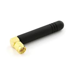
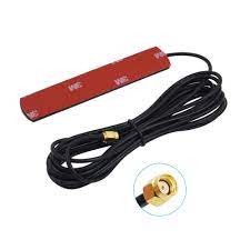
GSM Antenna Dlenp 2dbi/3dbi Patch Antenna with SMA Male Connector
- GSM Antenna
- Gain: 2 to 3dbi
- Wire Length: 3 metre
- 3dbi Sticker Antenna
- GSM Antenna
- SMA Male Connector
- Frequency Range(MHz): 824-960/1710-1990Mhz
- Bandwidth (MHz): 136/280
- VSWR≤1.5
- Gain(dB): 2-3dbi
- Max Input power(W): 60W
- Input Impedance: 50 Ω
- Polarization Type: Vertical
- Cable Type: RG174
- Mounting Adhesive
- Net weight: 47g

HX711–24 Bit Analog to Digital Converter (ADC)
- It is an ADC converter with two differential input channels
- An active-low noise PGA is integrated inside the chip which provides the gain of 32, 64 and 128
- It has a power-on-reset capability which simplifies digital interface initialization.
- All controls to the IC are made through the pins. Programming is not needed.
- You can select a data rate of 10SPS or 80SPS at the output.
- Provides simultaneous supply rejection of 50Hz and 60Hz supply.
- Built-in analog power supply regulator
- The voltage supply range is from 2.6V to 5.5V
- The temperature range is from -40 °C to +85℃
Reviews
There are no reviews yet.