
I am text block. Click edit button to change this text. Lorem ipsum dolor sit amet, consectetur adipiscing elit. Ut elit tellus, luctus nec ullamcorper mattis, pulvinar dapibus leo.
-25%

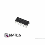
CD4099 8-Bit Addressable Latch IC
Original price was: ₹30.00.₹25.00Current price is: ₹25.00. inc. GST
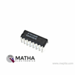
CD4043 CMOS Quad 3-State RS Latch IC
Original price was: ₹25.00.₹20.00Current price is: ₹20.00. inc. GST
CD4042 Quad Clocked D Latch IC
Original price was: ₹24.00.₹18.00Current price is: ₹18.00. inc. GST
- Quad Clocked D Latch
- Supply Voltage Range: 3 to 20V
- Input Current: ±10mA
- Power Dissipation: 200mW
- Low level Output Voltage: 0.05V
- High level Output Voltage Min.: 4.95V
- Low level Input Voltage Max.: 1.5V
- High level Input Voltage Min.: 3.5V
- Propagation Delay Time Max.: 500ns
- Package: DIP-16
- High noise immunity 0.45 VDD (typ.)
- Low power TTL compatibility Fan out of 2 driving 74L or 1 driving 74LS
- Clock polarity control
- Fully buffered data inputs
- Q and Q outputs
Description
CD4042 comprises of four clocked ‘‘D’’ latches, designed by using monolithic complementary MOS (CMOS) technology, integrated with P- and N-channel enhancement mode transistors.It consists of four latches having a common clock input, four buffered inputs and outputs pins. Each Latch inside CD4042 consists of 1 data input pin and two outputs Q and ~Q. The change in both outputs’ value depends on the clock level. In addition to these inputs, it also consist of polarity input which used to program the clock input.
The data present at the data input is transformed to Q when the polarity input remains LOW. The transfer occurs during the 1 clock level during the 0 clock level and when it is HIGH. The data is sent to the outputs at each clock transition, based on the polarity input. However, at the same clock level, the value remains constant until the clock signal value changes and becomes the polar opposite of the previous one.
The IC’s output is always packaged in a 16-pin dual inline hermetically sealed box (DIP). This IC also has good noise immunity, low thermal dissipation, and ESD protection, among other things. Low power consumption and a wide voltage supply range are two advantages of CMOS logic-based ICs. A D-type latch/flip-flop with two stable states designed as a timed latch. A D-type latch has a one-clock-cycle delay in its input. Delay circuits are frequently generated by cascading multiple D-type flip-flops, and are used in a variety of applications such as digital television systems. The D-type flip-flop is also known as a D flip-flop or a delay flip-flop.
Application
- Digital electronics for data storage
- Bounce elimination switch
- Computers use this IC for computing
- Buffer storage, data transfer, and holding registers
- Used as pulse latches for pulsing the clock quickly
- General Digital Logic
- Used in high circuit designs due to their fast speed
Reviews (0)
Shipping & Delivery

Related products


1/4W 5% Assorted Value Carbon Film Resistor Assortment Kit Set pack electronic diy kit
- 100% brand new and high quality.
- Fine workmanship and long service life.
- 1/4W carbon film resistor package.
- High precision and stability.
- Easy to use.
- Precision: 5%
- Error: 5%
- Values
- 10Ω, 15Ω, 22Ω, 33Ω, 47Ω, 68Ω, 100Ω, 220Ω, 330Ω, 470Ω, 1k, 1k5, 2k2, 3k3, 4k7, 5k6, 6K8, 8K2, 10K, 15K, 22K, 33K, 47K, 56K, 68K, 100K, 150K, 220K, 330K, 470K
- Package included: 150pcs

25pcs Button Switch Kit
- Relative Humidity: 95%
- Rated Voltage: 12V
- Rated Current: 50 mA
- Contact resistance: 50M Ohm Max (initial)
- The insulation resistance: 100M Ohm minDC (250V)
- The compressive strength: AC250V (50/60Hz for 1 minute)
- Mechanical life: 100000 cycles
- The environment temperature: 25° ~ + 105°
- The operating strength: 180/250 (plus or minus 30gf)
- Dimension: 12 * 12 * 7.3 round convex type
- Total Buttons: 25pcs
- Colours: 5 (Black, Red, White, Blue, Yellow)

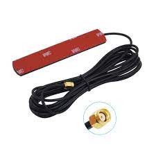
GSM Antenna Dlenp 2dbi/3dbi Patch Antenna with SMA Male Connector
- GSM Antenna
- Gain: 2 to 3dbi
- Wire Length: 3 metre
- 3dbi Sticker Antenna
- GSM Antenna
- SMA Male Connector
- Frequency Range(MHz): 824-960/1710-1990Mhz
- Bandwidth (MHz): 136/280
- VSWR≤1.5
- Gain(dB): 2-3dbi
- Max Input power(W): 60W
- Input Impedance: 50 Ω
- Polarization Type: Vertical
- Cable Type: RG174
- Mounting Adhesive
- Net weight: 47g
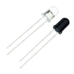
IR LED Sensor
- Size: 5mm LED
- Wavelength: 940nm wavelength (most commonly used)
- Forward current (IF) is 100mA (normal condition) and 300mA (max.)
- 5A of surge forward current
- 24v to 1.4v of forward voltage
- Temperature : -40 to 100 ℃
- Soldering Temperature should not exceed 260 ℃
- Power Dissipation of 150mW at 25℃ (free-air temperature) or below
- Spectral bandwidth of 45nm
- Viewing angle: 30 to 40 degree
- High Reliability
- Excessive radiant intensity
- Having lead spacing of 2.54mm
- Easy to use with breadboard or perf board
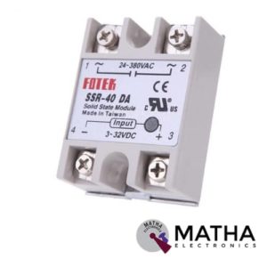

Solid State Relay SSR-40DD 40A 3-32V DC to 5-60V DC SSR 40DD Relay Solid State
- Model: SSR-40 DD.
- Control mode: DC-DC
- Input voltage: 3-32V DC.
- Output voltage: 5-60V DC.
- Output current: 40A.
- On voltage: ≤1v.
- One-off time: ≤10ms.
- Off leakage current: ≤2ma.
- Loading current: 40A
- Control current: 3-25mA DC
- Material: plastic + metal.
- Environment temperature: -30 to +75
- Long service life and high reliability.
- Reduced electromagnetic interference.
- Highly reliable, compact size designed to offer users maximum simplicity.
- Weight: 0. 106Kg.
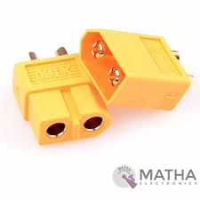
XT60 Connector
- Manufacturer: AMASS
- Connector Series: XT60H
- Rated Voltage: DC 500V
- Metal Material: Brass Gold Plated
- Rated Current: 30A
- Momentary Current: 60A
- Number of pins: 2
- Colour: Yellow
- Contact Resistance: 0.55mΩ
- FR Level: UL94 V0
- Use Times: 1000 TIMES
- Temperature: -20℃ to 120℃
- Spatial Orientation Straight
- Compatible for Wire size up to 12AWG
- Mechanical mounting for cable
- Electrical mounting soldered
- Contact plating Gold flash
Reviews
There are no reviews yet.