
I am text block. Click edit button to change this text. Lorem ipsum dolor sit amet, consectetur adipiscing elit. Ut elit tellus, luctus nec ullamcorper mattis, pulvinar dapibus leo.
-23%

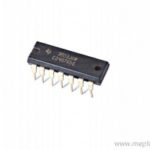
CD4078BE CMOS 8-Input NOR OR Gate IC
Original price was: ₹23.00.₹15.00Current price is: ₹15.00. inc. GST
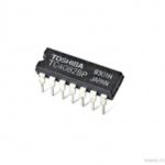
CD4082 Dual 4 Input AND Gate IC
Original price was: ₹22.00.₹15.00Current price is: ₹15.00. inc. GST
CD4081 Quad 2 Input AND Gate IC
Original price was: ₹26.00.₹20.00Current price is: ₹20.00. inc. GST
- Quad 2 Input AND Gate
- Supply Voltage Range: 3 to 20V
- Input Current: ±10mA
- Power Dissipation: 200mW
- No Of Inputs: 8
- No Of Outputs: 4
- Quiescent Current Max.: 5µA
- Low level Output Voltage: 0.05V
- High level Output Voltage Min.: 4.95V
- Low level Input Voltage Max.: 1.5V
- High level Input Voltage Min.: 3.5V
- Propagation Delay Time Max.: 250ns
- Package: DIP-14
Description
CD4081 belong to the CD4XXX IC series. This CD4081 designed as monolithic Quad 2 Input AND Gate designed by implementing the complementary MOS technology, integrated with P and N type enhancement mode transistors. The CD4081 IC operates at a wide range of working voltage, a wide range of working conditions. And directly interfaces with CMOS, NMOS, and TTL. The output of the IC always comes in TTL which makes it quite easy to function with other TTL devices and microcontrollers.
CD4081 offers features such as ESD barring and high noise immunity. Each output protected against static damage by using clamping diodes. CD4081 Operates at a supply voltage of range between 3V to 15V. This IC designed for operation over the full military temperature range of 0°C to 70°C. The IC CD4081 comes as smaller in size and offers much faster speed which makes it highly reliable in every kind of device. CD4081 IC can be soldered directly to the circuit board or easily mounted on a 14 pin IC base.
The CD4081 manufactured in 14-lead hermetic dual-in-line ceramic packages (F3A suffix), 14-lead dual-in-line plastic packages (E suffix), 14-lead small-outline packages (M, MT, M96, and NSR suffixes), and 14-lead thin shrink small-outline packages (PW and PWR suffixes).
The AND gate designed as a basic digital logic gate that implements logical conjunction. An AND gate operates on logical multiplication rules. If all the inputs to the AND gate are HIGH, then the output will be high. If none or not all inputs to the AND gate are HIGH, results in LOW output.
Application
- Measurement of frequency
- Enable gate and Inhibit gate
Reviews (0)
Shipping & Delivery

Related products
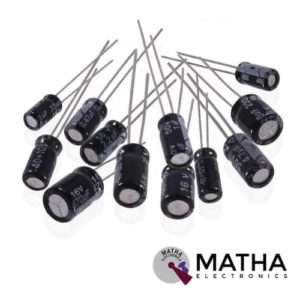


650NM Laser Diode
- Wavelength: 650nm
- Output optical power: 5mW
- Operating voltage: 5V
- Operating current: ~30mA
- Input current: 30mA
- Housing material: Copper
- Power lead length: 120mm.
- Transmit power: 58mW
- Spot: size 10mm to 15mm at 15meters
- Life span more than 2000 hours
- Driver circuit: APC circuit
- Small size
- Cost-effective
- Breadboard friendly
- Operating temperature -10°C to 40°C
- Dimension: :15mm x 6mm
- Weight: 10 grams
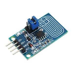
Capacitor Touch Dimmer, Constant Voltage LED Stepless Dimming, PWM Control Board
- Voltage range: 4V to 5V
- Maximum output current: 500mA
- Hole distance: 16 mm
- Aperture: 5 mm
- The lamp brightness can be adjusted by requirement, it is very to operate.
- It can touch in medium protection, such as glass, acrylic, plastic, ceramics, and so on, which is very safe.
- Anti power and phone interference, the EFT can reach above +/-2KV; the touch response sensitivity and reliability will not be affected by the close distance or multi-angle mobile phone interference.
- Dimming mode: Non-polar PWM dimming.
- PCB size: 23 x 20mm

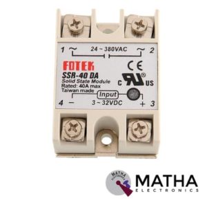
Solid State Relay Module DC To AC SSR-40DA 3-32VDC/24-380VAC 40A
- Control mode: DC-AC
- Input voltage: 3-32V DC.
- Output voltage: 24-380V AC.
- Output current: 40A.
- Working voltage: 250V.
- Material: plastic + metal.
- Loading current: 40A
- Control current: 3-25mA DC
- On voltage: ≤1.5V AC
- One-off Time: ≤10ms
- Off Leakage Current: ≤2mA
- Dielectrics voltage-resistance: 2500VAC
- Environment temperature: -30 to +75
- Long service life and high reliability.
- Reduced electromagnetic interference.
- Highly reliable, compact size designed to offer users maximum simplicity.
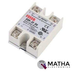
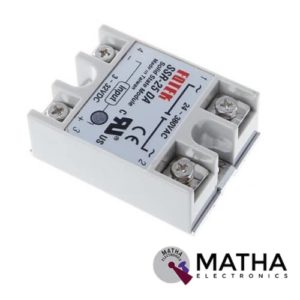
Solid State Relay Module SSR-25DA 25A /250V 3-32V DC Input 24-380VAC Output
- Control mode: DC-AC
- Input voltage: 3-32V DC.
- Output voltage: 24-380V AC.
- Output current: 25A.
- Working voltage: 250V.
- Material: plastic + metal.
- Environment temperature: -30 to +75
- Long service life and high reliability.
- Reduced electromagnetic interference.
- Highly reliable, compact size designed to offer users maximum simplicity.
- Dimension: 6. 5Cm x 4. 5Cm x 2. 2Cm


TP5100 4.2v 8.4v Single Double Lithium Battery Charge Management Li-ion Battery Compatible 2A Charging Board
- Input voltage: 5-15V DC power supply.
- Charge status: full and unloaded blue lights, charging red.
- Double 8.4v / 4.2v lithium rechargeable single .
- Programmable charge current. 0. 1A-2A .
- Programmable steady precharge current 10% -100%.
- Wide operating voltage, maximum reach I8V.
- Red and green LED charge status indicator.
- Chip temperature protection, overcurrent protection, under voltage protection.
- Battery temperature protection, reverse battery shutdown, short circuit protection.
- Switching frequency 400Khz, usable inductance 20uH and more.
- PWR_ON Power battery for switching control.
Reviews
There are no reviews yet.