
I am text block. Click edit button to change this text. Lorem ipsum dolor sit amet, consectetur adipiscing elit. Ut elit tellus, luctus nec ullamcorper mattis, pulvinar dapibus leo.
-17%

Back to products
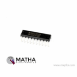
CD4042 Quad Clocked D Latch IC
Original price was: ₹24.00.₹18.00Current price is: ₹18.00. inc. GST
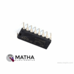
CD4099 8-Bit Addressable Latch IC
Original price was: ₹30.00.₹25.00Current price is: ₹25.00. inc. GST
- 8 Bit Addressable Latch
- Supply Voltage Range: 3 to 20V
- Input Current: ±10mA
- Power Dissipation : 200mW
- Quiescent Current Max. : 100µA
- Low level Output Voltage: 0.05V
- High-level Output Voltage Min.: 4.95V
- Low level Input Voltage Max.: 1.5V
- High level Input Voltage Min.: 3.5V
- Propagation Delay Time Max.: 450ns
- Package: DIP-16
Description
CD4099 IC belongs to the CD4000 IC series. CD4099 deigned as an 8 – bit addressable latch with three address inputs (A0–A2), a lively low enable input (E), active high clear input (CL), a data input (D), and eight outputs (Q0–Q7). Data is entered into a specific bit in the latch when that bit addressed by the address inputs and therefore the enable (E) is LOW. Data entry inhibited when enabling pin (E) remains HIGH. All outputs switch to LOW when clear pin (CL) and enable pin (E) are HIGH. Channel demultiplexing occurs when clear (CL) is HIGH and enable (E) is LOW. The bit that addressed offers a lively HIGH output that follows the info input while all unaddressed bits remain LOW. The IC offers many features like low thermal dissipation, high noise immunity, and operative flexibility in terms of workability voltages.
A digital logic circuit called an addressable latch is used to store a bit of digital data or a digital state. When the clock input is high, addressable latching logic circuits are prone to capturing, or ‘latching,’ the logic level existing on the data line. If the data on the D line changes state when the clock pulse is high, for example, the output, Q, follows the input, D, in a D-type latching circuit. The last state of the D input is caught and held within the latch when the CLK input falls to logic 0.
Application
Multi-line decoders
A/D converters
Reviews (0)
Shipping & Delivery

Related products


1/4W 5% Assorted Value Carbon Film Resistor Assortment Kit Set pack electronic diy kit
- 100% brand new and high quality.
- Fine workmanship and long service life.
- 1/4W carbon film resistor package.
- High precision and stability.
- Easy to use.
- Precision: 5%
- Error: 5%
- Values
- 10Ω, 15Ω, 22Ω, 33Ω, 47Ω, 68Ω, 100Ω, 220Ω, 330Ω, 470Ω, 1k, 1k5, 2k2, 3k3, 4k7, 5k6, 6K8, 8K2, 10K, 15K, 22K, 33K, 47K, 56K, 68K, 100K, 150K, 220K, 330K, 470K
- Package included: 150pcs

10 Segment Led Bargraph Light Display Red, Yellow, Green, Blue
- LED type: LED array bar
- Segments: 10
- LED Colour: Green
- Housing color: white
- Reverse voltage: 5V
- Forward Voltage - Typical: 1.85 V
- Forward Voltage - Maximum: 2.2 V
- DC forward current: 30mA
- Peak forward current: 175mA
- Power dissipation: 75mW
- Peak wavelength: 590nm
- Luminous Intensity Typical: 120 Mcd
- Operating temperature: -40°C to +85°C
- 10 Separately Controlled LED's
- High Brightness
- High-Intensity Green Output
- Ideal for Audio and Meter Displays
- Economically priced
- Easy to Mount
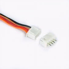
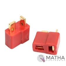
Dean Connector
- Male plug size: About 13* 7* 19mm
- Female plug size: About 13* 7* 15mm
- Current Rating: 30Amps
- Colour: Red and golden
- Material: Plastic and metal
- Provides a secure connection for battery and motor connections
- Eliminates the possibility of wrong polarity connections
- Used in RC hobby, car, boat, plane, helicopter, LIPO battery, etc.
- Dimension: 9x0.7x2cm
- Weight:20gm
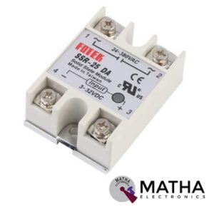
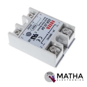
Solid State Relay Module SSR-25DA 25A /250V 3-32V DC Input 24-380VAC Output
- Control mode: DC-AC
- Input voltage: 3-32V DC.
- Output voltage: 24-380V AC.
- Output current: 25A.
- Working voltage: 250V.
- Material: plastic + metal.
- Environment temperature: -30 to +75
- Long service life and high reliability.
- Reduced electromagnetic interference.
- Highly reliable, compact size designed to offer users maximum simplicity.
- Dimension: 6. 5Cm x 4. 5Cm x 2. 2Cm


TP5100 4.2v 8.4v Single Double Lithium Battery Charge Management Li-ion Battery Compatible 2A Charging Board
- Input voltage: 5-15V DC power supply.
- Charge status: full and unloaded blue lights, charging red.
- Double 8.4v / 4.2v lithium rechargeable single .
- Programmable charge current. 0. 1A-2A .
- Programmable steady precharge current 10% -100%.
- Wide operating voltage, maximum reach I8V.
- Red and green LED charge status indicator.
- Chip temperature protection, overcurrent protection, under voltage protection.
- Battery temperature protection, reverse battery shutdown, short circuit protection.
- Switching frequency 400Khz, usable inductance 20uH and more.
- PWR_ON Power battery for switching control.
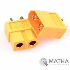
XT60 Connector
- Manufacturer: AMASS
- Connector Series: XT60H
- Rated Voltage: DC 500V
- Metal Material: Brass Gold Plated
- Rated Current: 30A
- Momentary Current: 60A
- Number of pins: 2
- Colour: Yellow
- Contact Resistance: 0.55mΩ
- FR Level: UL94 V0
- Use Times: 1000 TIMES
- Temperature: -20℃ to 120℃
- Spatial Orientation Straight
- Compatible for Wire size up to 12AWG
- Mechanical mounting for cable
- Electrical mounting soldered
- Contact plating Gold flash
Reviews
There are no reviews yet.