
I am text block. Click edit button to change this text. Lorem ipsum dolor sit amet, consectetur adipiscing elit. Ut elit tellus, luctus nec ullamcorper mattis, pulvinar dapibus leo.
-22%

CD4050 Hex Buffer or Converter IC
Original price was: ₹25.00.₹22.00Current price is: ₹22.00. inc. GST
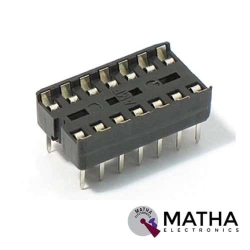
14 Pin IC Base
Original price was: ₹4.00.₹2.00Current price is: ₹2.00. inc. GST
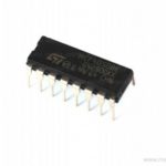
CD4502BE CMOS Strobed Hex Inverter Buffer IC
Original price was: ₹32.00.₹25.00Current price is: ₹25.00. inc. GST
- CMOS Strobed Hex Inverter/Buffer
- Number of Input Lines: 6
- Number of Output Lines: 6
- Polarity: Inverting
- High Level Output Current: -4.2 mA
- Logic Family: CD4000
- Low Level Output Current: 25.2 mA
- Maximum Power Dissipation: 100 mW
- Number of Channels per Chip: 5
- Output Type: 3-State
- Propagation Delay Time: 380 ns at 5 V, 180 ns at 10 V, 130 ns at 15 V
- Operating Temperature Range: -55°C to +125°C
- Supply Voltage Range: 3V to 18V
- Package: PDIP-16
Description
CD4502BE designed as a Strobed Hex Inverter (NOT gate) IC-based on monolithic complementary MOS (CMOS) technology. This IC come with six Inverter buffer inside it and provide 3 state output. This Converter IC widely used in buffer circuits and wave generator circuits.CD4049 ideal for use in high voltage applications as it offers a wide range of operating voltage from 3V to 18V. As it functions as an inverter IC and an inverter convert the logic level HIGH to LOW and LOW to HIGH. The IC also provides buffered outputs which improve transfer characteristics by providing very high gain. The CD4502BE IC manufactured in 16 – pin hermetically sealed dual in line package (DIP)ceramic (D) packages.
A Logic 1 in the OUTPUT DISABLE input produces a high impedance state in all six outputs. This feature allows the common busing of output thus simplifying system design. A logic 1 in the input INHIBIT switches the all 6 output to logic 0 if the output disables input 1 logic 0. Moreover, this inverter IC capable of driving 2 standard TTL load. Which is equivalent to a 6-time JDEC B series IL standard.
APPLICATION
- 3 State Hex Inverter for interfacing IC with data bus
- COS/MOS to TTL hex buffer
Reviews (0)
Shipping & Delivery

Related products


1/4W 5% Assorted Value Carbon Film Resistor Assortment Kit Set pack electronic diy kit
- 100% brand new and high quality.
- Fine workmanship and long service life.
- 1/4W carbon film resistor package.
- High precision and stability.
- Easy to use.
- Precision: 5%
- Error: 5%
- Values
- 10Ω, 15Ω, 22Ω, 33Ω, 47Ω, 68Ω, 100Ω, 220Ω, 330Ω, 470Ω, 1k, 1k5, 2k2, 3k3, 4k7, 5k6, 6K8, 8K2, 10K, 15K, 22K, 33K, 47K, 56K, 68K, 100K, 150K, 220K, 330K, 470K
- Package included: 150pcs

10 Segment Led Bargraph Light Display Red, Yellow, Green, Blue
- LED type: LED array bar
- Segments: 10
- LED Colour: Green
- Housing color: white
- Reverse voltage: 5V
- Forward Voltage - Typical: 1.85 V
- Forward Voltage - Maximum: 2.2 V
- DC forward current: 30mA
- Peak forward current: 175mA
- Power dissipation: 75mW
- Peak wavelength: 590nm
- Luminous Intensity Typical: 120 Mcd
- Operating temperature: -40°C to +85°C
- 10 Separately Controlled LED's
- High Brightness
- High-Intensity Green Output
- Ideal for Audio and Meter Displays
- Economically priced
- Easy to Mount


25pcs Button Switch Kit
- Relative Humidity: 95%
- Rated Voltage: 12V
- Rated Current: 50 mA
- Contact resistance: 50M Ohm Max (initial)
- The insulation resistance: 100M Ohm minDC (250V)
- The compressive strength: AC250V (50/60Hz for 1 minute)
- Mechanical life: 100000 cycles
- The environment temperature: 25° ~ + 105°
- The operating strength: 180/250 (plus or minus 30gf)
- Dimension: 12 * 12 * 7.3 round convex type
- Total Buttons: 25pcs
- Colours: 5 (Black, Red, White, Blue, Yellow)

5-36v Switch Drive High-power MOSFET Trigger Module
- Operating Voltage: DC 5V - 36V;
- The trigger source: digital high-low (DC3.3V - 20V), can be connected microcontroller IO port, PLC interfaces, DC power, you can access the PWM signal, the signal frequency 0--20KHZ perfect support.
- Output capacity: DC 5V - 36V, at room temperature, continuous current 15A, power 400W! Lower auxiliary cooling conditions, the maximum current up to 30A.
- Applications: You can control the output of power equipment, motors, light bulbs, LED lights, DC motors, micro-pumps, solenoid valves, etc.. You can enter
- PWM, motor speed control, lamp brightness.
- Availability: unlimited switch
- Operating temperature: -40-85
- Dimension: 34mm x 17mm x 12mm
- The use of imported dual-MOS parallel active output, lower resistance, more current, strong power at room temperature, 15A, 400W, to meet the most use of the equipment
- Wide voltage, the perfect support for PWM
- Easily control high power devices
- Input PWM to achieve motor speed control, lamp brightness control
Capacitor Touch Dimmer, Constant Voltage LED Stepless Dimming, PWM Control Board
- Voltage range: 4V to 5V
- Maximum output current: 500mA
- Hole distance: 16 mm
- Aperture: 5 mm
- The lamp brightness can be adjusted by requirement, it is very to operate.
- It can touch in medium protection, such as glass, acrylic, plastic, ceramics, and so on, which is very safe.
- Anti power and phone interference, the EFT can reach above +/-2KV; the touch response sensitivity and reliability will not be affected by the close distance or multi-angle mobile phone interference.
- Dimming mode: Non-polar PWM dimming.
- PCB size: 23 x 20mm
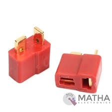
Dean Connector
- Male plug size: About 13* 7* 19mm
- Female plug size: About 13* 7* 15mm
- Current Rating: 30Amps
- Colour: Red and golden
- Material: Plastic and metal
- Provides a secure connection for battery and motor connections
- Eliminates the possibility of wrong polarity connections
- Used in RC hobby, car, boat, plane, helicopter, LIPO battery, etc.
- Dimension: 9x0.7x2cm
- Weight:20gm
Reviews
There are no reviews yet.