
I am text block. Click edit button to change this text. Lorem ipsum dolor sit amet, consectetur adipiscing elit. Ut elit tellus, luctus nec ullamcorper mattis, pulvinar dapibus leo.
-33%

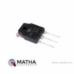
2SC2625 NPN Transistor 450V 10A
Original price was: ₹125.00.₹90.00Current price is: ₹90.00. inc. GST
2SC3281 NPN Transistor 200V 15A
Original price was: ₹113.00.₹75.00Current price is: ₹75.00. inc. GST
LF356 JFET Input Operational Amplifier IC
Original price was: ₹60.00.₹40.00Current price is: ₹40.00. inc. GST
- Input Offset Voltage: 10mV
- Input Offset Current Max: 50pA
- Input Bias Current Max: 200pA
- Common-Mode Rejection Ratio: 100dB
- Slew Rate: 12V/µs
- Package: DIP-8
Description
LF356 designed as a junction field effect transistor input operational amplifier IC. The IC features low input bias and offset currents/low offset voltage and offset voltage drift, coupled with offset adjust which does not degrade drift or common mode rejection. The IC is always available in an 8-pin dual in line hermetically sealed IC package (DIP). The LF356 offers a wide variety of working conditions, operating voltages, and is compatible with practically every TTL, CMOS, and PMOS device on the market. The IC also has a variety of properties, including a high input impedance and noise immunity.
The LF356 device is the first monolithic JFET input operational amplifier to combine well-matched, high-voltage JFETs with conventional bipolar transistors on the same chip (BI-FETTM Technology). Low input bias and offset currents/low offset voltage characterise these amplifiers. And there’s offset voltage drift with offset adjust, which doesn’t affect drift or common-mode rejection. High slew rate, wide bandwidth, exceptionally rapid settling time, low voltage and current noise, and a low 1/f noise corner are all features of the devices.
JFET (Junction field effect transistor) operational amplifier is a simple electronic configuration that boost up a voltage of lower strength to a higher level. Operational amplifier usually designed to used with external feedback components such as resistors and capacitors. Operational amplifiers also used in devices such as home theatre systems, VCRs, PCs, Laptops, etc.
Applications
- Precision High-Speed Integrators
- Fast D/A and A/D Converters
- High Impedance Buffers
- Wideband, Low Noise, Low Drift Amplifiers
- Logarithmic Amplifiers
- Photocell Amplifiers
- Sample and Hold Circuits
Reviews (0)
Shipping & Delivery

Related products

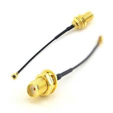
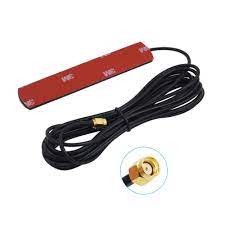
GSM Antenna Dlenp 2dbi/3dbi Patch Antenna with SMA Male Connector
- GSM Antenna
- Gain: 2 to 3dbi
- Wire Length: 3 metre
- 3dbi Sticker Antenna
- GSM Antenna
- SMA Male Connector
- Frequency Range(MHz): 824-960/1710-1990Mhz
- Bandwidth (MHz): 136/280
- VSWR≤1.5
- Gain(dB): 2-3dbi
- Max Input power(W): 60W
- Input Impedance: 50 Ω
- Polarization Type: Vertical
- Cable Type: RG174
- Mounting Adhesive
- Net weight: 47g

HX711–24 Bit Analog to Digital Converter (ADC)
- It is an ADC converter with two differential input channels
- An active-low noise PGA is integrated inside the chip which provides the gain of 32, 64 and 128
- It has a power-on-reset capability which simplifies digital interface initialization.
- All controls to the IC are made through the pins. Programming is not needed.
- You can select a data rate of 10SPS or 80SPS at the output.
- Provides simultaneous supply rejection of 50Hz and 60Hz supply.
- Built-in analog power supply regulator
- The voltage supply range is from 2.6V to 5.5V
- The temperature range is from -40 °C to +85℃
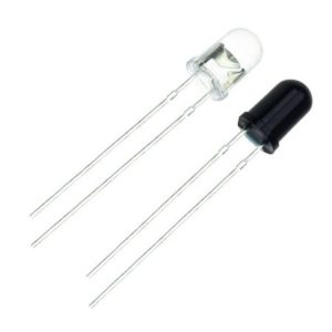
IR LED Sensor
- Size: 5mm LED
- Wavelength: 940nm wavelength (most commonly used)
- Forward current (IF) is 100mA (normal condition) and 300mA (max.)
- 5A of surge forward current
- 24v to 1.4v of forward voltage
- Temperature : -40 to 100 ℃
- Soldering Temperature should not exceed 260 ℃
- Power Dissipation of 150mW at 25℃ (free-air temperature) or below
- Spectral bandwidth of 45nm
- Viewing angle: 30 to 40 degree
- High Reliability
- Excessive radiant intensity
- Having lead spacing of 2.54mm
- Easy to use with breadboard or perf board

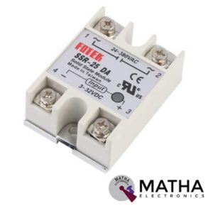
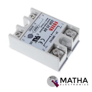
Solid State Relay Module SSR-25DA 25A /250V 3-32V DC Input 24-380VAC Output
- Control mode: DC-AC
- Input voltage: 3-32V DC.
- Output voltage: 24-380V AC.
- Output current: 25A.
- Working voltage: 250V.
- Material: plastic + metal.
- Environment temperature: -30 to +75
- Long service life and high reliability.
- Reduced electromagnetic interference.
- Highly reliable, compact size designed to offer users maximum simplicity.
- Dimension: 6. 5Cm x 4. 5Cm x 2. 2Cm


TP5100 4.2v 8.4v Single Double Lithium Battery Charge Management Li-ion Battery Compatible 2A Charging Board
- Input voltage: 5-15V DC power supply.
- Charge status: full and unloaded blue lights, charging red.
- Double 8.4v / 4.2v lithium rechargeable single .
- Programmable charge current. 0. 1A-2A .
- Programmable steady precharge current 10% -100%.
- Wide operating voltage, maximum reach I8V.
- Red and green LED charge status indicator.
- Chip temperature protection, overcurrent protection, under voltage protection.
- Battery temperature protection, reverse battery shutdown, short circuit protection.
- Switching frequency 400Khz, usable inductance 20uH and more.
- PWR_ON Power battery for switching control.
Reviews
There are no reviews yet.