
I am text block. Click edit button to change this text. Lorem ipsum dolor sit amet, consectetur adipiscing elit. Ut elit tellus, luctus nec ullamcorper mattis, pulvinar dapibus leo.
-34%

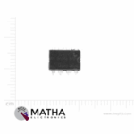
LF356 JFET Input Operational Amplifier IC
Original price was: ₹60.00.₹40.00Current price is: ₹40.00. inc. GST
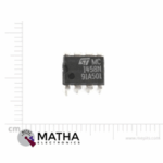
LM1458 Dual Operational Amplifier IC
Original price was: ₹23.00.₹15.00Current price is: ₹15.00. inc. GST
2SC3281 NPN Transistor 200V 15A
Original price was: ₹113.00.₹75.00Current price is: ₹75.00. inc. GST
- Collector-base Voltage: 200V
- Collector Current: 15A
- Transistor Polarity: NPN
- Total Power Dissipation:150W
- Current Gain max. : 160
- Transition Frequency: 10MHz
- Package: T0-247
Description
This 2SC3281 NPN bipolar transistor is specifically intended for use in low-power silicon NPN bipolar junction transistors. The 2SC3281 has a very low saturation voltage and excellent high gain performance. Within the operating range, the 2SC3281 is a three terminal NPN device. A voltage or current applied to one pair of transistor terminals controls the current flowing through another set of terminals. Because the regulated (output) power might be larger than the controlling (input) power, a transistor can amplify a signal.
The transistor is the most important component in an electrical circuit. In an NPN transistor, two pieces of P-type silicon (the base) are sandwiched between two pieces of N-type silicon (the collector and emitter). These transistors were designed to transmit electrons from the emitter to the collector (so conventional current flows from collector to emitter). The emitter “emits” electrons into the base, whereas the base regulates how many electrons the emitter emits. After interacting with the holes in the base, these electrons are transmitted to the collector. The collector “collects” the freed electrons and transfers them to the next portion of the circuit.
The main aim of the NPN transistor is to amplify weak signals that enter through the base and generate powerful amplify signals at the collector end. The travel of an electron in an NPN transistor is from the emitter to the collector area, resulting in current in the transistor. Because the bulk of charge carriers in such transistors are electrons, which have a higher mobility than holes, they are commonly utilised in circuits. The emitter, collector, and base of an NPN transistor are the three terminals. The centre part of an NPN transistor is weakly doped, and it is the most critical factor in the transistor’s operation. Meanwhile, the emitter was little doped, whereas the collector was extensively doped.
Reviews (0)
Shipping & Delivery

Related products


1/4W 5% Assorted Value Carbon Film Resistor Assortment Kit Set pack electronic diy kit
- 100% brand new and high quality.
- Fine workmanship and long service life.
- 1/4W carbon film resistor package.
- High precision and stability.
- Easy to use.
- Precision: 5%
- Error: 5%
- Values
- 10Ω, 15Ω, 22Ω, 33Ω, 47Ω, 68Ω, 100Ω, 220Ω, 330Ω, 470Ω, 1k, 1k5, 2k2, 3k3, 4k7, 5k6, 6K8, 8K2, 10K, 15K, 22K, 33K, 47K, 56K, 68K, 100K, 150K, 220K, 330K, 470K
- Package included: 150pcs


5-36v Switch Drive High-power MOSFET Trigger Module
- Operating Voltage: DC 5V - 36V;
- The trigger source: digital high-low (DC3.3V - 20V), can be connected microcontroller IO port, PLC interfaces, DC power, you can access the PWM signal, the signal frequency 0--20KHZ perfect support.
- Output capacity: DC 5V - 36V, at room temperature, continuous current 15A, power 400W! Lower auxiliary cooling conditions, the maximum current up to 30A.
- Applications: You can control the output of power equipment, motors, light bulbs, LED lights, DC motors, micro-pumps, solenoid valves, etc.. You can enter
- PWM, motor speed control, lamp brightness.
- Availability: unlimited switch
- Operating temperature: -40-85
- Dimension: 34mm x 17mm x 12mm
- The use of imported dual-MOS parallel active output, lower resistance, more current, strong power at room temperature, 15A, 400W, to meet the most use of the equipment
- Wide voltage, the perfect support for PWM
- Easily control high power devices
- Input PWM to achieve motor speed control, lamp brightness control

ADXL 335 Accelerometer IC
- 3-axis sensing
- Small, low profile package
- 4 mm × 4 mm × 1.45 mm LFCSP
- Low power : 350 μA (typical)
- Single-supply operation: 1.8 V to 3.6 V
- 10,000 g shock survival
- Excellent temperature stability
- BW adjustment with a single capacitor per axis
- RoHS/WEEE lead-free compliant
- 8V- 3.6V single-supply operation
- Integrated X, Y, and Z axis accelerometer on a single chip
- X and Y axis has a 0.5Hz to 1600Hz bandwidth
- Z axis has a 0.5Hz to 550Hz bandwidth
- Hermetically sealed for temp and humidity resistance


Dual Micro USB 3.7v to 5V 2A Power Bank DIY 18650 LiPo Charger
- 4-level LED lamp display power, not working state intelligent automatic shutdown;
- The built-in lithium battery protection IC, over-current, under-voltage protection;
- Dual USB output ports.
- Dimensions: 68 x 34 x 9 mm (LxWxH)
- Weight: 10 gm
- Input port: MicroUSB (Andro)
- Input requirements: 5V constant voltage power supply can do charge input power, the most matching charger for 5v1a above
- Output port: USB
- Output parameters: 5V1A/5V2A
- Requirements for rechargeable batteries:
- Compatible Batteries: 18650 batteries, cell phone batteries, flat-panel batteries, MP3 batteries, etc. 3.7v-4.2V polymer Lithium battery,
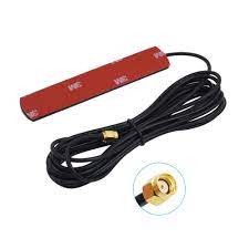
GSM Antenna Dlenp 2dbi/3dbi Patch Antenna with SMA Male Connector
- GSM Antenna
- Gain: 2 to 3dbi
- Wire Length: 3 metre
- 3dbi Sticker Antenna
- GSM Antenna
- SMA Male Connector
- Frequency Range(MHz): 824-960/1710-1990Mhz
- Bandwidth (MHz): 136/280
- VSWR≤1.5
- Gain(dB): 2-3dbi
- Max Input power(W): 60W
- Input Impedance: 50 Ω
- Polarization Type: Vertical
- Cable Type: RG174
- Mounting Adhesive
- Net weight: 47g

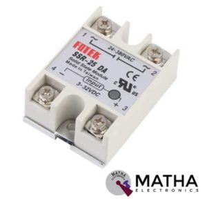
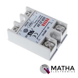
Solid State Relay Module SSR-25DA 25A /250V 3-32V DC Input 24-380VAC Output
- Control mode: DC-AC
- Input voltage: 3-32V DC.
- Output voltage: 24-380V AC.
- Output current: 25A.
- Working voltage: 250V.
- Material: plastic + metal.
- Environment temperature: -30 to +75
- Long service life and high reliability.
- Reduced electromagnetic interference.
- Highly reliable, compact size designed to offer users maximum simplicity.
- Dimension: 6. 5Cm x 4. 5Cm x 2. 2Cm
Reviews
There are no reviews yet.