
I am text block. Click edit button to change this text. Lorem ipsum dolor sit amet, consectetur adipiscing elit. Ut elit tellus, luctus nec ullamcorper mattis, pulvinar dapibus leo.
-10%


PAM8403 DIGITAL AMPLIFIER BOARD
Original price was: ₹100.00.₹50.00Current price is: ₹50.00. inc. GST
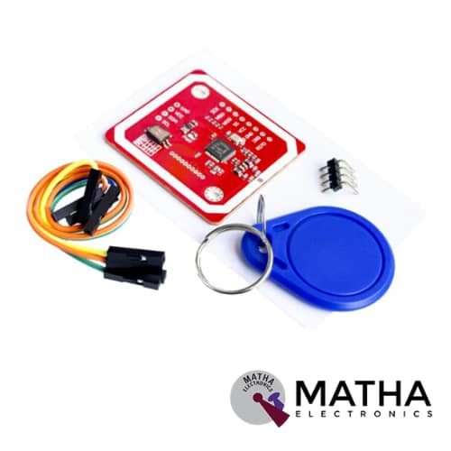
PN532 NFC MODULE
Original price was: ₹1,500.00.₹1,300.00Current price is: ₹1,300.00. inc. GST
PCF8591 ADC-DAC
Original price was: ₹500.00.₹450.00Current price is: ₹450.00. inc. GST
- Operating voltage range: 2.5V-6V
- Low standby current
- I2C bus serial input/output
- PCF8591 by 3 hardware address pins addressing
- PCF8591 I2C bus speed sampling rate decided 4 analogue inputs programmable single-ended or differential input
- Automatic incremental channel selection
- PCF8591 analogue voltage range from VSS to VDD
- On-chip track-and-hold circuit
- 8-bit successive approximation A / D converter
- 1 analogue output DAC gain
- Single power supply
- Module power supply indicator lights
- DA output indicator
- Dimension: 3.6*2.3cm
Description
PCF8591 ADC-DAC is a monolithically integrated, separate power supply, and low-power device. This is a breakout board with a single-chip, 8-bit CMOS data acquisition device for PCF8591 IC. The PCF8591 ADC-DAC consists of four analogue inputs and one analogue output. It communicates via a serial I2C bus interface. Three address pins A0, A1, and A2 are used in programming the hardware address. This allows the use of up to eight devices connected to the I²C‑bus without additional hardware.
Address, control, and data signals transmitted in serial via a two-wire bidirectional I2C bus. The maximum conversion rate determines the maximum speed of the I²C-bus. PCF8591 is an 8 bit analogue to digital or 8 bit digital to analogue converter module which can read analogue values up to 256. LDR and thermistor circuit is provided on the board. This indicates the precise value of light intensity and temperature of the module. There are SCL and SDA pins for serial clock and serial data address which requires 2.5-6V supply voltage. As a result, provides a low standby current in the I2C bus interface.
The knob of the potentiometer adjusts the input voltage on the module. There are also three jumpers on the board J4, J5, J6. J4 is connected to select the thermistor access circuit, J5 to select the LDR/photoresistor access circuit, and J6 to select the adjustable voltage access circuit. Two LEDs in the module indicates the output voltage intensity and the intensity of the supply voltage. So higher the output or supply voltage gives the high intensity of the LED. These LEDs can also test using a potentiometer on VCC or on an AOUT pin. PCF8591 features analogue input multiplexing, on-chip track and hold function, 8-bit analogue-to-digital conversion, and an 8‑bit digital-to-analogue conversion.
Reviews (0)
Shipping & Delivery

Related products
1 CHANNEL 12V RELAY
- 1-Channel relay interface board
- Operating voltage: 12V DC
- Provide high current relay of 15A
- For quick and easy connection high-quality screw terminals provided
- Can control both AC & DC appliances
- LED status indicates relay ON/OFF state.
- High current relay of 10A @250 V AC/10A@ 30V DC
- Standard interface that can be controlled by a microcontroller (Arduino, 8051, PIC, AVR, DSP, ARM)
- For easy accessibility input signal pin connected to burg sticks
- Dimension: 43*17*17mm
- Weight: 150gm


4*3 MATRIX KEYPAD
- Operating voltage: 12V DC
- The maximum voltage across each button: 24v
- The maximum current across each button: 3mA
- Ultra-thin design
- Adhesive backing provides easy integration
- Easy communication with any microcontroller
- Flexible
- Only 7 microcontroller pins required to access 12 keys
- High price-performance ratio
- Allows microcontroller to scan 8 output pins to check which 16 button
- Long life
- Maximum operating temperature: 0 degrees to 50 degrees Celsius
- Dimension: 70*77*1mm
- Weight: 7.5gm

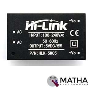
AC-DC Power Module HLK-5M05 230V to 5V /5W
- Meet UL, CE requirements
- Rated input voltage: AC 100V -230V
- Input voltage range: 90V -264V AC
- Maximum input current: <0.2A
- Input current surge: <10A
- Maximum input voltage: <270V AC
- Input Low Voltage Efficiency: Vin=110V AC,Output full-load≥ 69%
- Input High Voltage Efficiency: Vin=220V AC,output full-load≥ 70 %
- Long-term reliability
- Voltage Regulation: ±0.2%
- Load Regulation: ±0.5%
- Ultra-thin and small module
- High efficiency, high power density
- Low ripple and low noise
- Output overload and short circuit protection
- Working temperature: – 20 degrees to +60 degrees Celsius
- Storage temperature: -40 degrees to 80 degrees Celsius
- Relative humidity: 5-95%
- Cooling way: Natural cooling
- Atmospheric pressure: 80-106Kpa
- Weight: 21g
- Size: 38x23x18mm
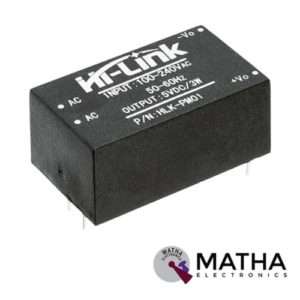
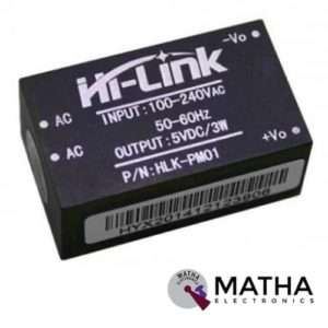
AC-DC Power Module HLK-PM01 230V to 5V /3W
- Meet UL, CE requirements
- Rated input voltage: AC 100V -230V
- Maximum input voltage: <270V AC
- Voltage Regulation: ±0.2%
- Load Regulation: ±0.5%
- High efficiency, high power density
- Ultra-thin and small module
- Low ripple and low noise
- Output overload and short circuit protection
- 100% load ageing and testing
- The product is designed to meet the requirements of the EMC and Safety Test
- Low power consumption, environmental protection, no-load loss <0.1W
- High efficiency, high power density
- Working temperature: – 20 degrees to +60 degrees Celsius
- Storage temperature: + 80-40 -degree
- Relative humidity: 5-95%
- Cooling way: Natural cooling
- Atmospheric pressure: 80-106Kpa
- Weight: 21g
- Size: 38x23x18mm
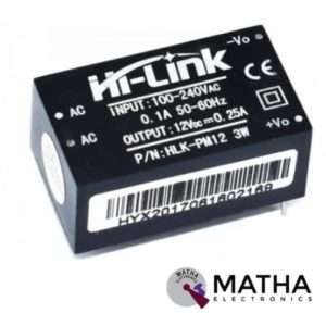

AC-DC Power Module HLK-PM12 230V to 12V /3W
- Rated input voltage: AC 100V -230V
- Input voltage range: 90V -264V AC
- Maximum input current: <0.2A
- Input current surge: <10A
- Maximum input voltage: <270V AC
- Input Low Voltage Efficiency Vin=110V AC,Output full-load≥ 69%
- Input High Voltage Efficiency Vin=220V AC,output full-load≥ 70 %
- Short-term maximum output current: ≥1000 mA
- Long-term reliability
- Voltage Regulation: ±0.2%
- Load Regulation: ±0.5%
- Ultra-thin and small module
- High efficiency, high power density
- Low ripple and low noise
- Output overload and short circuit protection
- Working temperature: – 20 degrees to +60 degrees Celsius
- Storage temperature: -40 degrees to 80 degrees Celsius
- Relative humidity: 5-95%
- Cooling way: Natural cooling
- Atmospheric pressure: 80-106Kpa
- Weight: 21g
- Size: 38x23x18mm


DS3231 RTC MODULE
- Operating voltage of DS3231: 2.3 v to 5.5v
- 400Khz I2C interface
- Automatic power failure battery switch circuitry
- RTC counts seconds, minutes, hours, and year
- High precision clock chip DS3231
- Programmable square-wave output
- Chip temperature sensor accuracy:+/_3 degree Celsius
- Memory chip: AT24C32 with 32K storage capacity
- CR2032 battery backup with a high life span
- Low power consumption
- Register for ageing trim
- Dimension: 38mm*22mm*14mm
Reviews
There are no reviews yet.