
What is Microblaze Processor : Architecture, Working & Its Applications
The MicroBlaze processor was created in 2002 to incorporate a number of complex features to fulfill both new and expanding market demand. Therefore, the MicroBlaze processor is a crucial component of Xilinx’s Low-End Portfolio for enabling faster system development with Artix®-7 FPGAs, Spartan®-6, and Zynq®-7000 AP SoCs. This processor is highly programmable, allowing it to be used as an embedded processor or microcontroller within FPGAs and as a co-processor in ARM Cortex-A9-based Zynq-7000 AP SoCs. This article provides an overview of the MicroBlaze processor’s architecture and application compatibility.
What is Microblaze Processor?
MicroBlaze is the name of Xilinx’s soft microprocessor that is primarily designed for FPGAs. This processor is simply implemented in Xilinx FPGAs’ general-purpose memory and logic fabric. This processor is related to the RISC-based DLX architecture and includes a flexible connection system to serve a variety of embedded applications. MicroBlaze’s primary I/O bus and AXI connection are memory-mapped transaction buses with a master-slave facility.
MicroBlaze makes use of a specialised LMB bus to access local memory and offers rapid on-chip storage. This processor’s cache size, pipeline depth, memory management unit, embedded peripherals, and bus interfaces are configurable by the user.

Microblaze Features
- It has 32-bit instruction words including 2 addressing modes & 3 operands.
- The address bus is 32-bit.
- It has 3 stage pipeline or a 5-stage pipeline.
- An ALU block unit with a shifter.
- Harvard architecture includes 32-bit data and address bus.
- Data interface & LMB or local memory bus instruction.
- AX14 and AX14 stream interfaces.
- Floating point unit & memory management unit.
- It supports lockstep.
- Debug & trace interface.
Microbaze Architecture
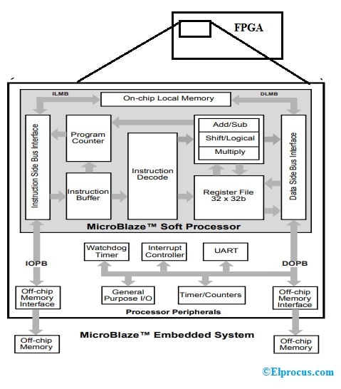
Below is a block diagram of the MicroBlaze processor. This MicroBlaze processor supports over 70 design possibilities and is highly customizable. This design includes both fixed and customizable hardware components, such as the Instruction or Data Cache, the Memory Management Unit, the Floating-Point Unit, etc.
A MicroBlaze-based embedded system consists primarily of MicroBlaze Soft Processor Core, On-chip Local Memory, Standard Bus Interconnects, and OPB Peripherals (On-chip Peripheral Bus). A MicroBlaze processing system ranges from a single processor core with local memory to a huge system with many MicroBlaze processors, external memory, and numerous OPB peripherals.
Microblaze Processor Architecture
Soft Processor Core
The MicroBlaze soft processor core is crucial to the MicroBlaze embedded system. This is an extremely quick and effective 32-bit RISC processor with the following characteristics:
- The instruction set is Orthogonal.
- Separate data & instruction buses.
- 32-bit general purpose registers.
- It has an optional complete 32-bit barrel shifter.
- Inbuilt interfaces to fast OCM or on-chip memory & IBM’s industry-standard OPB (On-chip Peripheral Bus).
On-chip Local Memory
The synchronous memory is a local memory used primarily to enable on-chip Block RAM.
Standard Bus Interconnects
The instruction and data side bus interfaces include an interface to local memory dubbed LMB (Local Memory Bus) and an interface to IBM’s On-chip Peripheral Bus. So that we can create systems that strictly adhere to Harvard architecture, we can use a single OPB in conjunction with a bus arbiter to distribute resources.
The local memory bus provides guaranteed single-cycle access to on-chip block RAM. This highly efficient, straightforward, single-master bus protocol is ideal for interacting with rapid local memory. The On-chip Peripheral Bus (OPB) is a 32-bit wide multi-master bus that is ideal for connecting peripherals and external memory to the MicroBlaze processor’s core.
On-chip Peripheral Bus Peripherals
OPB peripherals complete the MicroBlaze hardware system by providing various functions, including Watchdog Timer or Timebase, General purpose Timer or Counters, IC (Interrupt Controller), and various controllers, including SRAM, Flash Memory, ZBT Memory, BRAM, DDR, SDRAM, UART Lite, SPI, I2C, General purpose I/O, UART 16450/550, and Ethernet 10/100 MAC. In addition, we can add and define peripherals primarily for new functions, or an interface to an existing FPGA design.
Microblaze Instruction Set
The instruction sets of Microblaze include arithmetic, logic, branch, load/store, and others. The size of each instruction is constant. No more than three registers may be specified as operands. Below are examples of Microblaze’s Type A and Type B instruction forms.
Register-register instructions are often formatted with Type A instructions. Also included are a single destination register and two source registers. The Type B instruction structure is mostly utilised for register-immediate instructions, which consist of the opcode, a single destination and source register, and a 16-bit immediate value source.
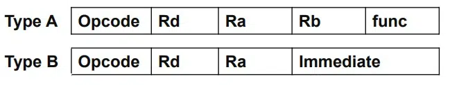
In the above two instruction formats, the opcode is an operation code, Rd is a destination register that is encoded with 5-bits, Ra & Rb are source registers where each encoded with 5-bits and Immediate is a 16-bit value.
Arithmetic Instructions
The type A and Type B arithmetic instructions are given below.
Type A
| ADD Rd, Ra, Rbadd | Rd = Ra+Rb, Carry flag affected |
| ADD K Rd, Ra, RbAdd and keep carry | Rd = Ra+Rb, Carry flag not affected |
| RSUB Rd, Ra, RbReverse subtract | Rd = R-Rb, Carry flag not affected |
Type B
| ADD I Rd, Ra, Immadd immediate | Rd = Ra+signExtend32 (Imm) |
| ADD IK Rd, Ra, Immadd immediate and keep carry | Rd = Ra+ signExtend32 (Imm) |
| RSUBIK Rd, Ra, Immreverse subtract with immediate | Rd = Ra+ signExtend32 (Imm) -Ra |
| SRA Rd, Raarithmetic shift right | Rd = (Ra>>1) |
Logic Instructions
The type A and Type B logic instructions are given below.
Type A
| OR Rd, Ra, RbLogical or | Rd = Ra | Rb |
| AND Rd,Ra, RbLogical add | Rd = Ra & Rb |
| XOR Rd, Ra, RbLogoical xor | Rd = Rb ^ Rb |
| ANDN Rd, Ra, RbLogical and not | Rd = Ra & (Rb) |
Type B
| ORI Rd, Ra, Immlogical OR with immediate | Rd = Ra | signExtend32 (Imm) |
| ANDI Rd, Ra, Immlogical AND with immediate | Rd = Ra & signExtend32 (Imm) |
| XORI Rd, Ra, Immlogoical XOR with immediate | Rd = Ra ^ signExtend32 (Imm) |
| ANDNI Rd, Ra, ImmLogical AND NOT with immediate | Rd = Ra & (signExtend32 (Imm)) |
Branch Instructions- Unconditional
Modify the Program Counter register
| BRID Immbranch immediate with immediate delay | PC = PC+ signExtend32 (Imm)allow delay slot execution |
| BRLID Rd, Immbranch and link immediate with immediate delay (function call) | Rd = PCPC = PC+& signExtend32 (Imm)allow delay slot execution |
| RTSD Ra, Immreturn from subroutine | PC = Ra + signExtend32 (Imm)allow delay slot execution |
| RTID Ra, Immreturn from interrupt | PC = Ra + signExtend32 (Imm)allow delay slot executionset interrupt enable in MSR |
Branch Instructions- Unconditional1
Change the Program Counter register when a condition is satisfied
| BEQI Ra, Immbranch if equal | PC = PC+ signExtend32 (Imm)If Ra = = 0 |
| BREI Ra, Immbranch if not equal | Rd = PCPC = PC+& signExtend32 (Imm)If Ra! = 0 |
Branch Instructions- Unconditional2
Change the Program Counter register when a condition is satisfied
| BLTI Ra, Immbranch if lower than | PC = PC+ signExtend32 (Imm)If Ra < 0 |
| BLEI Ra, Immbranch if lower equal than | Rd = PCPC = PC+& signExtend32 (Imm)If Ra!< = 0 |
| BGTI Ra, Immbranch if greater than | PC = PC+ signExtend32 (Imm)If Ra!> 0 |
| BGEI Ra, Immbranch if greater equal than | PC = PC+signExtend32 (Imm)If Ra!>= 0 |
Load/Store Instructions -Type A
| LW Rd, Ra, RbLoad word | Address = Ra+RbRd = *Address |
| SW Rd, Ra, RbStore word | Address – Ra+Rb*Address = Rd |
Type B
| LWI Rd, Ra, ImnLoad word immediate | Address = Ra + signExtend32 (Imm)Rd = *Address |
| SW Rd, Ra, ImmStore word immediate | Address = Ra + signExtend32 (Imm)*Address = Rd |
Other Instructions
| IMM, Immediate | Extend the Imm of a preceding type B instruction to 32-bits. |
| MFS Rd, SaMove from special-purpose register | Rd = SaSa- special purpose register, source operand |
| MTS Sd, RaMove to special purpose register | Sd = RaSd – special purpose register, destination operand |
- Registers
MicroBlaze processor architecture is totally orthogonal, with 32-bit general purpose registers and 32-bit special purpose registers, such as Program Counter and Machine Status Register.
- Pipeline Architecture
MicroBlaze’s pipeline architecture consists of fetch, decode, and complete stages. Hardware determines automatically the data forwarding, branching, and pipeline stalls.
- Load or Store Architecture
MicroBlaze supports three memory sizes: 8 bits (Byte), 16 bits (Halfword), and 32 bits (Word) (Word). Thus, memory accesses are always data-size aligned. This is a Big-Endian processor that accesses memory using the address of the Big-Endian address and labelling rules.
- Interrupts
When an interrupt occurs, this processor terminates the current instruction to manage the interrupt request by branching to the interrupt vector address and storing the instruction address to be executed. By deleting the IE (Interrupt Enablement) flag within the MSR, this processor will cease future interrupts (Machine Status Register).
How Does Microblaze Work?
The MicroBlaze processor offers 32-bit bus width, and its processor core is a RISC-based engine with a register file based on 32-bit LUT RAM and distinct memory & data access instructions.
This CPU merely supports both internal and external memory. All peripherals employ the identical CoreConnect OPB bus, hence the peripherals of the Virtex-II Pro CPU are well-matched with those of the IBM PowerPC.
The MicroBlaze processor gives you the entire freedom to select the memory, peripheral, and interface characteristics that will provide you with the exact system you need on a single FPGA at a lower price.
Microblaze Advantages
- It is cost-effective.
- It’s incredibly customizable.
- Its performance is superior to that of ARM.
- There is an embedded development kit to support it.
- It is a microprocessor with a soft core.
- This processor contains three fixed configurations that correspond to well-known processor classes to help you easily organize your programme: microcontroller, real-time, and application processor.
Microblaze Applications
- This processor satisfies numerous application specifications, including Industrial, Automotive, Medical, Consumer, etc.
- MicroBlaze’s applications span from basic software-based state machines to complicated controllers utilized in embedded applications or Internet-connected appliances.
- It is optimized for embedded applications such as industrial control, office automation, and automotive applications.
- The MicroBlaze is able to communicate with a vast array of peripherals, making it suitable for medium-scale applications.
- This processor’s malleable nature makes it adaptable to a variety of applications, allowing designers to exchange features for size to satisfy price and performance objectives for medical, automotive, industrial, and security applications.