
I am text block. Click edit button to change this text. Lorem ipsum dolor sit amet, consectetur adipiscing elit. Ut elit tellus, luctus nec ullamcorper mattis, pulvinar dapibus leo.
-29%

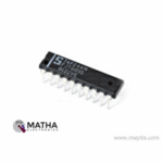
74F244 Octal Buffer or Driver IC With 3-State Output
Original price was: ₹85.00.₹55.00Current price is: ₹55.00. inc. GST
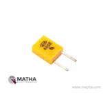
480 MHz 2 Pin Crystal Oscillator
Original price was: ₹45.00.₹30.00Current price is: ₹30.00. inc. GST
74366N Tri-State Hex Buffer IC
Original price was: ₹85.00.₹60.00Current price is: ₹60.00. inc. GST
- Tri-State Hex Buffer
- High-level output voltage: 3.1V
- Low-level output voltage: 0.4V
- High-level output current: -5.2mA
- Low-level output current: 32mA
- Input clamp voltage: -1.5V
- Propagation delay time max: 90ns
- Typical power dissipation: 295mW
- Supply voltage range: 4.75 to 5.25V
- Package: DIP-16
Description
A buffer designed basically as a logic gate that passes its input, unchanged, to its output. The main function of a buffer is to regenerate the input, usually using a strong high and a strong low. A buffer has one input and one output, in which its output is always equal to its input. Buffers are also used to increase the propagation delay of circuits by driving the large capacitive loads. Whereas the Line drivers designed as a special type of buffer that has the ability to drive a transmission line or cable that may be quite long. They also have the ability to adapt the input logic format to the specific line driving standard. These IC generally used to isolate other gates or circuit stages from each other. Thereby preventing the impedance of one circuit from affecting the impedance of another circuit.
74366N device is designed explicitly to improve both the performance and density of 3-state memory address drivers, clock drivers, and bus-oriented receivers and transmitters. 74366N Tri-State Hex Buffer IC is identical to the standard versions and offers a propagation delay time of 90ns. This IC operates at a supply voltage at a range between 4.75V and to a maximum of 5.25V. This IC is designed for operation over the full military temperature range of −0°C to 75°C. 74366N Tri-State Hex Buffer IC manufactured in 16−pin plastic PDIP wide-body surface-mount packages.
Applications
- Telecom Infrastructure mm
- TVs
- Set Top Boxes
- Network Switches
- Wireless Infrastructure
- Electronic Points of Sale
Reviews (0)
Shipping & Delivery

Related products


5-36v Switch Drive High-power MOSFET Trigger Module
- Operating Voltage: DC 5V - 36V;
- The trigger source: digital high-low (DC3.3V - 20V), can be connected microcontroller IO port, PLC interfaces, DC power, you can access the PWM signal, the signal frequency 0--20KHZ perfect support.
- Output capacity: DC 5V - 36V, at room temperature, continuous current 15A, power 400W! Lower auxiliary cooling conditions, the maximum current up to 30A.
- Applications: You can control the output of power equipment, motors, light bulbs, LED lights, DC motors, micro-pumps, solenoid valves, etc.. You can enter
- PWM, motor speed control, lamp brightness.
- Availability: unlimited switch
- Operating temperature: -40-85
- Dimension: 34mm x 17mm x 12mm
- The use of imported dual-MOS parallel active output, lower resistance, more current, strong power at room temperature, 15A, 400W, to meet the most use of the equipment
- Wide voltage, the perfect support for PWM
- Easily control high power devices
- Input PWM to achieve motor speed control, lamp brightness control


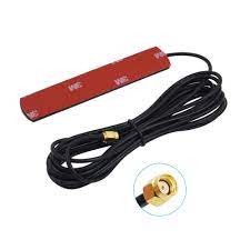
GSM Antenna Dlenp 2dbi/3dbi Patch Antenna with SMA Male Connector
- GSM Antenna
- Gain: 2 to 3dbi
- Wire Length: 3 metre
- 3dbi Sticker Antenna
- GSM Antenna
- SMA Male Connector
- Frequency Range(MHz): 824-960/1710-1990Mhz
- Bandwidth (MHz): 136/280
- VSWR≤1.5
- Gain(dB): 2-3dbi
- Max Input power(W): 60W
- Input Impedance: 50 Ω
- Polarization Type: Vertical
- Cable Type: RG174
- Mounting Adhesive
- Net weight: 47g

HX711–24 Bit Analog to Digital Converter (ADC)
- It is an ADC converter with two differential input channels
- An active-low noise PGA is integrated inside the chip which provides the gain of 32, 64 and 128
- It has a power-on-reset capability which simplifies digital interface initialization.
- All controls to the IC are made through the pins. Programming is not needed.
- You can select a data rate of 10SPS or 80SPS at the output.
- Provides simultaneous supply rejection of 50Hz and 60Hz supply.
- Built-in analog power supply regulator
- The voltage supply range is from 2.6V to 5.5V
- The temperature range is from -40 °C to +85℃


TP5100 4.2v 8.4v Single Double Lithium Battery Charge Management Li-ion Battery Compatible 2A Charging Board
- Input voltage: 5-15V DC power supply.
- Charge status: full and unloaded blue lights, charging red.
- Double 8.4v / 4.2v lithium rechargeable single .
- Programmable charge current. 0. 1A-2A .
- Programmable steady precharge current 10% -100%.
- Wide operating voltage, maximum reach I8V.
- Red and green LED charge status indicator.
- Chip temperature protection, overcurrent protection, under voltage protection.
- Battery temperature protection, reverse battery shutdown, short circuit protection.
- Switching frequency 400Khz, usable inductance 20uH and more.
- PWR_ON Power battery for switching control.
Reviews
There are no reviews yet.