
I am text block. Click edit button to change this text. Lorem ipsum dolor sit amet, consectetur adipiscing elit. Ut elit tellus, luctus nec ullamcorper mattis, pulvinar dapibus leo.
-32%

74HC147 10-to-4 Line Priority Encoder IC
Original price was: ₹42.00.₹35.00Current price is: ₹35.00. inc. GST
FS10KM Power Mosfet 60V 10A
Original price was: ₹76.00.₹60.00Current price is: ₹60.00. inc. GST
74HC139 Dual 2-Line to 4-Line Decoder Demultiplexer IC
Original price was: ₹22.00.₹15.00Current price is: ₹15.00. inc. GST
- Dual 2-Line to 4-Line Decoder/Demultiplexer
- Logic Family: HC
- Output Current Max: 5.2mA
- Power Dissipation: 320 mW
- No. of Pins: 16
- Operating Temperature Range: -40°C to +85°C
- Supply Voltage Range: 2V to 6V
- Package: DIP-16
Description
The 74HC139 designed to decodes two binary weighted address inputs (nA0, nA1) to four mutually exclusive outputs (nY0 to nY3). Each decoder features an enable input (nE). When nE remains HIGH all outputs forced HIGH. The enable input can be used as the data input for a 1-to-4 demultiplexer application. Inputs include clamp diodes. This enables the use of current limiting resistors to interface inputs to voltages in excess of VCC
The SN74HC139 is a high-performance memory decoding or data-routing device with extremely short propagation delay times. This decoder can reduce the consequences of system decoding in high-performance memory systems. When used with high-speed memories that use a quick enable circuit, the decoder’s delay time and the memory’s enable time are usually less than the memory’s typical access time. This indicates that the decoder’s effective system delay is negligible. In a single package, the SN74HC139 has two independent 2-line to 4-line decoders. As a result, in demultiplexing applications, the active-low enable (G) input is used as a data line. Meanwhile, each of the decoder/completely demultiplexer’s buffered inputs represents only one normalised load to its driving circuit.
A demultiplexer is a combinational logic circuit that switches a single common input line to one of numerous distinct output lines. The data distributor, often known as a Demultiplexer or “Demux,” is a device that distributes data. In a nutshell, this is the polar opposite of the Multiplexer from the last tutorial. The demultiplexer takes a single input data line and switches it one at a time to any of a number of distinct output lines. A serial data signal is fed into the demultiplexer, which converts it to parallel data on the output lines.
Reviews (0)
Shipping & Delivery

Related products

10 Segment Led Bargraph Light Display Red, Yellow, Green, Blue
- LED type: LED array bar
- Segments: 10
- LED Colour: Green
- Housing color: white
- Reverse voltage: 5V
- Forward Voltage - Typical: 1.85 V
- Forward Voltage - Maximum: 2.2 V
- DC forward current: 30mA
- Peak forward current: 175mA
- Power dissipation: 75mW
- Peak wavelength: 590nm
- Luminous Intensity Typical: 120 Mcd
- Operating temperature: -40°C to +85°C
- 10 Separately Controlled LED's
- High Brightness
- High-Intensity Green Output
- Ideal for Audio and Meter Displays
- Economically priced
- Easy to Mount


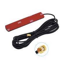
GSM Antenna Dlenp 2dbi/3dbi Patch Antenna with SMA Male Connector
- GSM Antenna
- Gain: 2 to 3dbi
- Wire Length: 3 metre
- 3dbi Sticker Antenna
- GSM Antenna
- SMA Male Connector
- Frequency Range(MHz): 824-960/1710-1990Mhz
- Bandwidth (MHz): 136/280
- VSWR≤1.5
- Gain(dB): 2-3dbi
- Max Input power(W): 60W
- Input Impedance: 50 Ω
- Polarization Type: Vertical
- Cable Type: RG174
- Mounting Adhesive
- Net weight: 47g
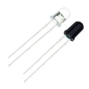
IR LED Sensor
- Size: 5mm LED
- Wavelength: 940nm wavelength (most commonly used)
- Forward current (IF) is 100mA (normal condition) and 300mA (max.)
- 5A of surge forward current
- 24v to 1.4v of forward voltage
- Temperature : -40 to 100 ℃
- Soldering Temperature should not exceed 260 ℃
- Power Dissipation of 150mW at 25℃ (free-air temperature) or below
- Spectral bandwidth of 45nm
- Viewing angle: 30 to 40 degree
- High Reliability
- Excessive radiant intensity
- Having lead spacing of 2.54mm
- Easy to use with breadboard or perf board
Reviews
There are no reviews yet.