
I am text block. Click edit button to change this text. Lorem ipsum dolor sit amet, consectetur adipiscing elit. Ut elit tellus, luctus nec ullamcorper mattis, pulvinar dapibus leo.
-25%


CD4007 Dual Complementary Pair Plus Inverter IC
Original price was: ₹30.00.₹20.00Current price is: ₹20.00. inc. GST

DS1302 Trickle Charge Timekeeping Chip IC
Original price was: ₹45.00.₹35.00Current price is: ₹35.00. inc. GST
74LS112 Dual J-K Negative Edge Triggered Flip-Flop IC
Original price was: ₹20.00.₹15.00Current price is: ₹15.00. inc. GST
- Dual JK Negative Edge Triggered Flip-Flops With Preset and Clear
- High-level input voltage: 2V
- Low-level input voltage: 0.8V
- High-level output current: -0.4mA
- Low-level output current: 8mA
- Maximum clock frequency: 45MHz
- Propagation delay time: 20ns
- Supply voltage range: 4.75 to 5.25V
- Package: DIP-16
Description
74LS112 dual JK flip-flop features individual J, K, clock, and asynchronous set and clear inputs to every flip-flop. It comprises of two independent negative-edge-triggered J-K flip-flops with individual J-K, clock, and direct clear inputs. The 74LS112 IC features a wide selection of working voltage, a good range of working conditions, and directly interfaces with CMOS, NMOS, and TTL. Moreover, output of IC always comes in TTL which makes it easy to figure with other TTL devices and microcontrollers.
Meanwhile, the J and K data is processed by the flip-flop on the falling fringe of the clock pulse. The clock triggering occurs at a voltage level and isn’t directly associated with the transition time of the falling edge of the clock pulse. Data on the J and K inputs could also be changed while the clock is HIGH or LOW without affecting the outputs as long because the setup and hold times are not violated. Meanwhile, a low logic level on the preset or clear inputs will set or reset the outputs no matter the logic levels of the opposite inputs.
The JK Flip Flop designed as a gated RS flip flop with the addition of the clock input circuitry. When both the inputs S and R are capable logic “1”, the invalid condition takes place. In order to prevent this invalid condition, a clock circuit is introduced. Moreover, the JK Flip Flop comprises of four possible input combinations thanks to the addition of the clocked input. The four inputs are “logic 1”, ‘logic 0”. “No change’ and “Toggle”.
Applications
- PCs and notebooks
- Digital Electronics
- Shift Registers
Reviews (0)
Shipping & Delivery

Related products


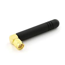
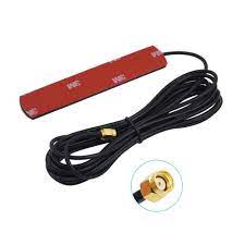
GSM Antenna Dlenp 2dbi/3dbi Patch Antenna with SMA Male Connector
- GSM Antenna
- Gain: 2 to 3dbi
- Wire Length: 3 metre
- 3dbi Sticker Antenna
- GSM Antenna
- SMA Male Connector
- Frequency Range(MHz): 824-960/1710-1990Mhz
- Bandwidth (MHz): 136/280
- VSWR≤1.5
- Gain(dB): 2-3dbi
- Max Input power(W): 60W
- Input Impedance: 50 Ω
- Polarization Type: Vertical
- Cable Type: RG174
- Mounting Adhesive
- Net weight: 47g


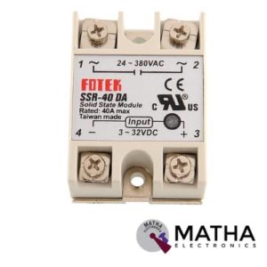
Solid State Relay Module DC To AC SSR-40DA 3-32VDC/24-380VAC 40A
- Control mode: DC-AC
- Input voltage: 3-32V DC.
- Output voltage: 24-380V AC.
- Output current: 40A.
- Working voltage: 250V.
- Material: plastic + metal.
- Loading current: 40A
- Control current: 3-25mA DC
- On voltage: ≤1.5V AC
- One-off Time: ≤10ms
- Off Leakage Current: ≤2mA
- Dielectrics voltage-resistance: 2500VAC
- Environment temperature: -30 to +75
- Long service life and high reliability.
- Reduced electromagnetic interference.
- Highly reliable, compact size designed to offer users maximum simplicity.
Reviews
There are no reviews yet.