
I am text block. Click edit button to change this text. Lorem ipsum dolor sit amet, consectetur adipiscing elit. Ut elit tellus, luctus nec ullamcorper mattis, pulvinar dapibus leo.
-45%

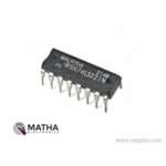
74LS221 Dual Monostable Multivibrator IC with Schmitt-Trigger Inputs
Original price was: ₹20.00.₹15.00Current price is: ₹15.00. inc. GST
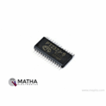
PT2323 6-Channel Audio Selector SMD IC
Original price was: ₹145.00.₹120.00Current price is: ₹120.00. inc. GST
BD135 NPN Transistor 45V 1.5A
Original price was: ₹11.00.₹6.00Current price is: ₹6.00. inc. GST
- Collector-base Voltage: 45V
- Collector Current: 1.5A
- Transistor Polarity: NPN
- Total Power Dissipation: 12.5W
- Current Gain max. : 250
- Package: T0-126
Description
This BD135 NPN bipolar transistor designed explicitly for use in general-purpose low power silicon NPN bipolar junction transistors. The BD135 offers exceptional high gain performance along with a very low saturation voltage. BD135 comes in a three terminal NPN device within the working range. The collector current IC is a function of the base current IB. Any change in the base current cause corresponding amplified change in collector current for a given collector emitter voltage VCE.
The most crucial component in an electrical circuit is the transistor. Two pieces of P-type silicon (the base) are placed between two pieces of N-type silicon in an NPN transistor (the collector and emitter). The main purpose of these transistors was to transport electrons from the emitter to the collector (so conventional current flows from collector to emitter). The emitter “emits” electrons into the base, and the base controls the amount of electrons the emitter emits. These electrons are transferred to the collector after mixing with the holes in the base. The collector “collects” and sends the bulk of the liberated electrons to the next section of the circuit.
The purpose of the NPN transistor is to amplify weak signals that enter the base and create powerful amplify signals at the collector end. The travel of an electron in an NPN transistor is from the emitter to the collector area, resulting in current in the transistor. Because the bulk of charge carriers in such transistors are electrons, which have a higher mobility than holes, they are commonly utilised in circuits. The emitter, collector, and base of an NPN transistor are the three terminals. The centre part of an NPN transistor is weakly doped, and it is the most critical factor in the transistor’s operation. Meanwhile, the emitter was little doped, whereas the collector was extensively doped.
Reviews (0)
Shipping & Delivery

Related products


650NM Laser Diode
- Wavelength: 650nm
- Output optical power: 5mW
- Operating voltage: 5V
- Operating current: ~30mA
- Input current: 30mA
- Housing material: Copper
- Power lead length: 120mm.
- Transmit power: 58mW
- Spot: size 10mm to 15mm at 15meters
- Life span more than 2000 hours
- Driver circuit: APC circuit
- Small size
- Cost-effective
- Breadboard friendly
- Operating temperature -10°C to 40°C
- Dimension: :15mm x 6mm
- Weight: 10 grams

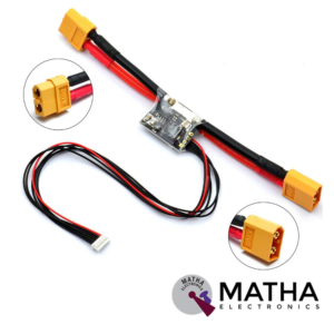
APM/Pixhawk Power Module V6.0 Output BEC 3A XT60 Plug 28V 90A
- Input Voltage Range: 6-28V DC
- Output voltage: 5.3V ± 0.1V
- Maximum output current: 3A
- Maximum current: 90A
- Maximum voltage: 30V
- Supports from 2 cell to 6 cell battery.
- 6P cable can be directly connected to APM/Pixhawk flight control
- Additional 4P rows of pin-free to wire/PIN to connect to another flight control
- Voltage and current measurement configured for 5V ADC.
- Switching regulator outputs 5.3V and 3A max.
- Dimensions: 25mm x 21mm x 9mm
- Weight: 17gm

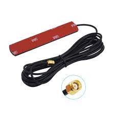
GSM Antenna Dlenp 2dbi/3dbi Patch Antenna with SMA Male Connector
- GSM Antenna
- Gain: 2 to 3dbi
- Wire Length: 3 metre
- 3dbi Sticker Antenna
- GSM Antenna
- SMA Male Connector
- Frequency Range(MHz): 824-960/1710-1990Mhz
- Bandwidth (MHz): 136/280
- VSWR≤1.5
- Gain(dB): 2-3dbi
- Max Input power(W): 60W
- Input Impedance: 50 Ω
- Polarization Type: Vertical
- Cable Type: RG174
- Mounting Adhesive
- Net weight: 47g

HX711–24 Bit Analog to Digital Converter (ADC)
- It is an ADC converter with two differential input channels
- An active-low noise PGA is integrated inside the chip which provides the gain of 32, 64 and 128
- It has a power-on-reset capability which simplifies digital interface initialization.
- All controls to the IC are made through the pins. Programming is not needed.
- You can select a data rate of 10SPS or 80SPS at the output.
- Provides simultaneous supply rejection of 50Hz and 60Hz supply.
- Built-in analog power supply regulator
- The voltage supply range is from 2.6V to 5.5V
- The temperature range is from -40 °C to +85℃
Reviews
There are no reviews yet.