
I am text block. Click edit button to change this text. Lorem ipsum dolor sit amet, consectetur adipiscing elit. Ut elit tellus, luctus nec ullamcorper mattis, pulvinar dapibus leo.
-29%
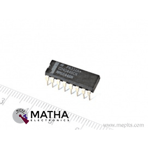
CD4043 CMOS Quad 3-State RS Latch IC
Original price was: ₹25.00.₹20.00Current price is: ₹20.00. inc. GST
7412N Triple 3-Input Positive NAND Gate IC
Original price was: ₹20.00.₹15.00Current price is: ₹15.00. inc. GST
CD4044 CMOS Quad 3-State RS Latch IC
Original price was: ₹21.00.₹15.00Current price is: ₹15.00. inc. GST
- CMOS Quad 3-State RS Latch
- Number of Circuits: 1
- Logic Type: CMOS
- Logic Family: CD4000
- Polarity: Non-Inverting
- Number of Input Lines/Output Lines: 8/4
- High Level Output Current: – 4.2 mA
- Propagation Delay Time: 350 ns at 5 V, 175 ns at 10 V, 120 ns at 15 V
- Supply Voltage Range: 3 to 15V
- Operating Temperature Range: – 55 C to + 125 C
- Package: PDIP 16
Description
CD4044 designed quad cross-coupled 3-STATE CMOS NAND latches. That mean it comes with four R-S latches, made by using the CMOS NAND logical gate. There exist a common 3-STATE ENABLE input for all four latches. Each latch in the IC consists of a separate Q output and individual SET and RESET inputs. The Q outputs controlled via a common ENABLE input. A logic “1” or high on the ENABLE input connects the latch states to the Q outputs. And also a logic “0” or low on the ENABLE input disconnects the latch states from the Q outputs. This results in an open circuit feature that allow common busing of the outputs. Meanwhile, this IC has many features such as high noise immunity, ESD barring, and excellent thermal overload protection. Meanwhile, CD4044 operates at a DC Supply Voltage Range, (VDD) f -0.5V to +18V.
An SR latch, also known as an SR Flip-Flop, is a logic circuit with two inputs (S and R) and two outputs (Q and Q’). The status of output Q determines the state of this latch. When Q is 1 (High), the latch is said to be SET, and when Q is 0 (Low), the latch is said to be RESET. Two cross-coupled NAND gates or two cross-coupled NOR gates are used to create an SR latch or flip flop.
Application
- Multiple bus storage
- Strobed register
- Four bits of independent storage with output enable
- General digital logic
Reviews (0)
Shipping & Delivery

Related products





HX711–24 Bit Analog to Digital Converter (ADC)
- It is an ADC converter with two differential input channels
- An active-low noise PGA is integrated inside the chip which provides the gain of 32, 64 and 128
- It has a power-on-reset capability which simplifies digital interface initialization.
- All controls to the IC are made through the pins. Programming is not needed.
- You can select a data rate of 10SPS or 80SPS at the output.
- Provides simultaneous supply rejection of 50Hz and 60Hz supply.
- Built-in analog power supply regulator
- The voltage supply range is from 2.6V to 5.5V
- The temperature range is from -40 °C to +85℃

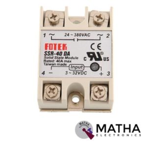
Solid State Relay Module DC To AC SSR-40DA 3-32VDC/24-380VAC 40A
- Control mode: DC-AC
- Input voltage: 3-32V DC.
- Output voltage: 24-380V AC.
- Output current: 40A.
- Working voltage: 250V.
- Material: plastic + metal.
- Loading current: 40A
- Control current: 3-25mA DC
- On voltage: ≤1.5V AC
- One-off Time: ≤10ms
- Off Leakage Current: ≤2mA
- Dielectrics voltage-resistance: 2500VAC
- Environment temperature: -30 to +75
- Long service life and high reliability.
- Reduced electromagnetic interference.
- Highly reliable, compact size designed to offer users maximum simplicity.
Reviews
There are no reviews yet.