
I am text block. Click edit button to change this text. Lorem ipsum dolor sit amet, consectetur adipiscing elit. Ut elit tellus, luctus nec ullamcorper mattis, pulvinar dapibus leo.
-32%

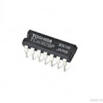
CD4085BE CMOS Dual 2-Wide 2-Input AND-OR-INVERT Gate IC
Original price was: ₹22.00.₹15.00Current price is: ₹15.00. inc. GST
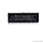
74HC138 3-Line to 8-Line Decoder Demultiplexer IC
Original price was: ₹45.00.₹35.00Current price is: ₹35.00. inc. GST
CD4086 CMOS Expandable 4 Wide 2 Input AND OR INVERT Gate IC
Original price was: ₹22.00.₹15.00Current price is: ₹15.00. inc. GST
- CMOS Expandable 4 Wide 2 Input AND OR INVERT Gate
- Supply Voltage Range: 3 to 18V
- Input Current: ±10mA
- Power Dissipation: 500mW
- Quiescent Current Max.: 20µA
- Low level Output Voltage Max.: 0.05V
- High level Output Voltage Min.: 4.95V
- Low-level Input Voltage Max.: 1.5V
- High-level Input Voltage Min.: 3.5V
- Propagation Delay Time Max.: 620ns
- Package: DIP-14
Description
CD4086 designed with one 4 Wide 2 Input AND OR INVERT Gate IC with one INHIBIT/EXP’ and an ENABLE /EXP input. For a 4 -wide AOI function INHIBIT/EXP’ connected to Vss and ENABLE /EXP to VDD. It helps to achieve a wide power supply operating range, low power consumption, and high noise margin. This device contains two independent combinations of gates each of which performs the logic AND-OR-INVERT function. The IC also comes as smaller in size and offers much faster speed. Thus makes it highly reliable in every kind of device.
CD4086 Operates at a supply voltage of range between 3V to 18V. This IC designed for operation over the full military temperature range of -55°C to 125°C.All inputs come with protection circuits against static discharge and transient excess voltage. The CD4085BE manufactured in 14-lead hermetic dual-in-line ceramic packages (F3A suffix), 14-lead dual-in-line plastic packages (E suffix), 14-lead small-outline packages (M, MT, M96, and NSR suffixes), and 14-lead thin shrink small-outline packages (PW and PWR suffixes). Moreover, it offers a power dissipation at a range of 500mW.
AND-OR-Invert (AOI) logic and AOI gates designed as two-level compound (or complex) logic functions made up of the combination of 1 or more AND gates followed by a NOR gate. The construction of AOI cells is especially efficient using CMOS technology. Where the entire number of transistor gates are often compared to an equivalent construction using NAND logic or NOR logic. The complement of AOI Logic is OR-AND-Invert (OAI) logic where the OR gates precede a NAND circuit.
Reviews (0)
Shipping & Delivery

Related products


1/4W 5% Assorted Value Carbon Film Resistor Assortment Kit Set pack electronic diy kit
- 100% brand new and high quality.
- Fine workmanship and long service life.
- 1/4W carbon film resistor package.
- High precision and stability.
- Easy to use.
- Precision: 5%
- Error: 5%
- Values
- 10Ω, 15Ω, 22Ω, 33Ω, 47Ω, 68Ω, 100Ω, 220Ω, 330Ω, 470Ω, 1k, 1k5, 2k2, 3k3, 4k7, 5k6, 6K8, 8K2, 10K, 15K, 22K, 33K, 47K, 56K, 68K, 100K, 150K, 220K, 330K, 470K
- Package included: 150pcs

10 Segment Led Bargraph Light Display Red, Yellow, Green, Blue
- LED type: LED array bar
- Segments: 10
- LED Colour: Green
- Housing color: white
- Reverse voltage: 5V
- Forward Voltage - Typical: 1.85 V
- Forward Voltage - Maximum: 2.2 V
- DC forward current: 30mA
- Peak forward current: 175mA
- Power dissipation: 75mW
- Peak wavelength: 590nm
- Luminous Intensity Typical: 120 Mcd
- Operating temperature: -40°C to +85°C
- 10 Separately Controlled LED's
- High Brightness
- High-Intensity Green Output
- Ideal for Audio and Meter Displays
- Economically priced
- Easy to Mount

ADXL 335 Accelerometer IC
- 3-axis sensing
- Small, low profile package
- 4 mm × 4 mm × 1.45 mm LFCSP
- Low power : 350 μA (typical)
- Single-supply operation: 1.8 V to 3.6 V
- 10,000 g shock survival
- Excellent temperature stability
- BW adjustment with a single capacitor per axis
- RoHS/WEEE lead-free compliant
- 8V- 3.6V single-supply operation
- Integrated X, Y, and Z axis accelerometer on a single chip
- X and Y axis has a 0.5Hz to 1600Hz bandwidth
- Z axis has a 0.5Hz to 550Hz bandwidth
- Hermetically sealed for temp and humidity resistance


Dual Micro USB 3.7v to 5V 2A Power Bank DIY 18650 LiPo Charger
- 4-level LED lamp display power, not working state intelligent automatic shutdown;
- The built-in lithium battery protection IC, over-current, under-voltage protection;
- Dual USB output ports.
- Dimensions: 68 x 34 x 9 mm (LxWxH)
- Weight: 10 gm
- Input port: MicroUSB (Andro)
- Input requirements: 5V constant voltage power supply can do charge input power, the most matching charger for 5v1a above
- Output port: USB
- Output parameters: 5V1A/5V2A
- Requirements for rechargeable batteries:
- Compatible Batteries: 18650 batteries, cell phone batteries, flat-panel batteries, MP3 batteries, etc. 3.7v-4.2V polymer Lithium battery,

HX711–24 Bit Analog to Digital Converter (ADC)
- It is an ADC converter with two differential input channels
- An active-low noise PGA is integrated inside the chip which provides the gain of 32, 64 and 128
- It has a power-on-reset capability which simplifies digital interface initialization.
- All controls to the IC are made through the pins. Programming is not needed.
- You can select a data rate of 10SPS or 80SPS at the output.
- Provides simultaneous supply rejection of 50Hz and 60Hz supply.
- Built-in analog power supply regulator
- The voltage supply range is from 2.6V to 5.5V
- The temperature range is from -40 °C to +85℃
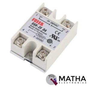
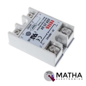
Solid State Relay Module SSR-25DA 25A /250V 3-32V DC Input 24-380VAC Output
- Control mode: DC-AC
- Input voltage: 3-32V DC.
- Output voltage: 24-380V AC.
- Output current: 25A.
- Working voltage: 250V.
- Material: plastic + metal.
- Environment temperature: -30 to +75
- Long service life and high reliability.
- Reduced electromagnetic interference.
- Highly reliable, compact size designed to offer users maximum simplicity.
- Dimension: 6. 5Cm x 4. 5Cm x 2. 2Cm


TP5100 4.2v 8.4v Single Double Lithium Battery Charge Management Li-ion Battery Compatible 2A Charging Board
- Input voltage: 5-15V DC power supply.
- Charge status: full and unloaded blue lights, charging red.
- Double 8.4v / 4.2v lithium rechargeable single .
- Programmable charge current. 0. 1A-2A .
- Programmable steady precharge current 10% -100%.
- Wide operating voltage, maximum reach I8V.
- Red and green LED charge status indicator.
- Chip temperature protection, overcurrent protection, under voltage protection.
- Battery temperature protection, reverse battery shutdown, short circuit protection.
- Switching frequency 400Khz, usable inductance 20uH and more.
- PWR_ON Power battery for switching control.
Reviews
There are no reviews yet.