
I am text block. Click edit button to change this text. Lorem ipsum dolor sit amet, consectetur adipiscing elit. Ut elit tellus, luctus nec ullamcorper mattis, pulvinar dapibus leo.

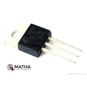
TOP223Y Offline PWM Switcher IC
Original price was: ₹120.00.₹100.00Current price is: ₹100.00. inc. GST
TOP243PN Off-line Switcher IC
- Supply Current: 1.6 mA
- Supply voltage range: 85-265VAC
- Power: 25W
- Output Voltage: 12 V
- Switching Frequency: 132 kHz
- Package: TO-DIP-8
- Extended power range for higher power applications
- No heatsink required up to 34 W using P/G packages.
- Features eliminate or reduce cost of external components.
- Fully integrated soft-start for minimum stress/overshoot.
- Externally programmable accurate current limit.
- Wider duty cycle for more power, smaller input capacitor .
- Separate line sense and current limit pins on Y/R/F packages
Description
TOPSwitch-GX family introduced by Power Integrations uses the same proven topology as TOPSwitch. This switcher IC comprises of high voltage power MOSFET, PWM control, fault protection, and other control circuitry integrated into a single CMOS chip. Various new functions are employed in this IC to reduce system cost and improve design flexibility, performance and energy efficiency.
Based on package type, either 1 or 3 additional pins over the TOPSwitch standard DRAIN, SOURCE and CONTROL terminals allow the certain features such as line sensing (OV/UV, line feed-forward/DCMAX reduction), accurate externally set current limit, remote ON/OFF. Moreover, it also offers a synchronization to an external lower frequency, and frequency selection (132 kHz/66 kHz). All package types offers the subsequent transparent features such as Soft-start, 132 kHz switching frequency (automatically reduced at light load), frequency jittering for lower EMI. And also provides wider DCMAX, hysteretic thermal shutdown, and bigger creepage packages. Moreover, all critical parameters ( current limit, frequency, PWM gain) provides tighter temperature and absolute tolerances to simplify design and optimize system cost.
These IC functions as a switched-mode power supply chip that converts a current at control input to a duty cycle at the open-drain output of high voltage power MOSFET. During normal functioning of the IC, the duty cycle of the power MOSFET reduces linearly with increase in CONTROL pin current.
Moreover, the TOPSwitch IC features, high voltage start-up, the cycle-by-cycle current limiting, loop compensation circuitry, auto-restart, thermal shutdown. And also the TOPSwitch-GX comprises of wide range of additional features that minimize system cost, increase power supply performance and style flexibility. A patented high voltage CMOS technology allows both the high voltage power MOSFET and every one the low voltage control circuitry to affordably integrated onto one monolithic chip.
Reviews (0)
Shipping & Delivery

Related products

5-36v Switch Drive High-power MOSFET Trigger Module
- Operating Voltage: DC 5V - 36V;
- The trigger source: digital high-low (DC3.3V - 20V), can be connected microcontroller IO port, PLC interfaces, DC power, you can access the PWM signal, the signal frequency 0--20KHZ perfect support.
- Output capacity: DC 5V - 36V, at room temperature, continuous current 15A, power 400W! Lower auxiliary cooling conditions, the maximum current up to 30A.
- Applications: You can control the output of power equipment, motors, light bulbs, LED lights, DC motors, micro-pumps, solenoid valves, etc.. You can enter
- PWM, motor speed control, lamp brightness.
- Availability: unlimited switch
- Operating temperature: -40-85
- Dimension: 34mm x 17mm x 12mm
- The use of imported dual-MOS parallel active output, lower resistance, more current, strong power at room temperature, 15A, 400W, to meet the most use of the equipment
- Wide voltage, the perfect support for PWM
- Easily control high power devices
- Input PWM to achieve motor speed control, lamp brightness control


ADXL 335 Accelerometer IC
- 3-axis sensing
- Small, low profile package
- 4 mm × 4 mm × 1.45 mm LFCSP
- Low power : 350 μA (typical)
- Single-supply operation: 1.8 V to 3.6 V
- 10,000 g shock survival
- Excellent temperature stability
- BW adjustment with a single capacitor per axis
- RoHS/WEEE lead-free compliant
- 8V- 3.6V single-supply operation
- Integrated X, Y, and Z axis accelerometer on a single chip
- X and Y axis has a 0.5Hz to 1600Hz bandwidth
- Z axis has a 0.5Hz to 550Hz bandwidth
- Hermetically sealed for temp and humidity resistance
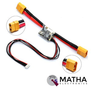
APM/Pixhawk Power Module V6.0 Output BEC 3A XT60 Plug 28V 90A
- Input Voltage Range: 6-28V DC
- Output voltage: 5.3V ± 0.1V
- Maximum output current: 3A
- Maximum current: 90A
- Maximum voltage: 30V
- Supports from 2 cell to 6 cell battery.
- 6P cable can be directly connected to APM/Pixhawk flight control
- Additional 4P rows of pin-free to wire/PIN to connect to another flight control
- Voltage and current measurement configured for 5V ADC.
- Switching regulator outputs 5.3V and 3A max.
- Dimensions: 25mm x 21mm x 9mm
- Weight: 17gm

HX711–24 Bit Analog to Digital Converter (ADC)
- It is an ADC converter with two differential input channels
- An active-low noise PGA is integrated inside the chip which provides the gain of 32, 64 and 128
- It has a power-on-reset capability which simplifies digital interface initialization.
- All controls to the IC are made through the pins. Programming is not needed.
- You can select a data rate of 10SPS or 80SPS at the output.
- Provides simultaneous supply rejection of 50Hz and 60Hz supply.
- Built-in analog power supply regulator
- The voltage supply range is from 2.6V to 5.5V
- The temperature range is from -40 °C to +85℃

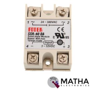
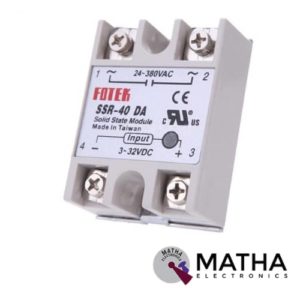
Solid State Relay Module DC To AC SSR-40DA 3-32VDC/24-380VAC 40A
- Control mode: DC-AC
- Input voltage: 3-32V DC.
- Output voltage: 24-380V AC.
- Output current: 40A.
- Working voltage: 250V.
- Material: plastic + metal.
- Loading current: 40A
- Control current: 3-25mA DC
- On voltage: ≤1.5V AC
- One-off Time: ≤10ms
- Off Leakage Current: ≤2mA
- Dielectrics voltage-resistance: 2500VAC
- Environment temperature: -30 to +75
- Long service life and high reliability.
- Reduced electromagnetic interference.
- Highly reliable, compact size designed to offer users maximum simplicity.

Solid State Relay SSR-40DD 40A 3-32V DC to 5-60V DC SSR 40DD Relay Solid State
- Model: SSR-40 DD.
- Control mode: DC-DC
- Input voltage: 3-32V DC.
- Output voltage: 5-60V DC.
- Output current: 40A.
- On voltage: ≤1v.
- One-off time: ≤10ms.
- Off leakage current: ≤2ma.
- Loading current: 40A
- Control current: 3-25mA DC
- Material: plastic + metal.
- Environment temperature: -30 to +75
- Long service life and high reliability.
- Reduced electromagnetic interference.
- Highly reliable, compact size designed to offer users maximum simplicity.
- Weight: 0. 106Kg.
Reviews
There are no reviews yet.