
I am text block. Click edit button to change this text. Lorem ipsum dolor sit amet, consectetur adipiscing elit. Ut elit tellus, luctus nec ullamcorper mattis, pulvinar dapibus leo.
-18%
80C52 Microcontroller IC
Original price was: ₹80.00.₹60.00Current price is: ₹60.00. inc. GST
2N2222A NPN Metal Transistor 75V 0.8A
Original price was: ₹22.00.₹15.00Current price is: ₹15.00. inc. GST
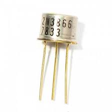
2N3866 NPN High Frequency Transistor 55V 0.4A
Original price was: ₹98.00.₹80.00Current price is: ₹80.00. inc. GST
- Type Designator: 2N3866
- Material of Transistor: Si
- Polarity: NPN
- Maximum Collector Power Dissipation (Pc): 5 W
- Maximum Collector-Base Voltage |Vcb|: 55 V
- Maximum Collector-Emitter Voltage |Vce|: 30
- Maximum Emitter-Base Voltage |Veb|: 3
- Maximum Collector Current |Ic max|: 0.4 A
- Max. Operating Junction Temperature (Tj): 200 °C
- Transition Frequency (ft): 500 MHz
- Collector Capacitance (Cc): 3 p
- Forward Current Transfer Ratio (hFE), MIN: 10
- Total Power Dissipation: 5W
- Transition Frequency: 500MHz
- Package: T0-39
Description
The 2N3866 is a TO-38 packaging transistor built specifically for RF applications. The maximum collector dissipation of this IC is 5 watts, and the maximum transition frequency is 500 MHz. In the VHF and UHF band areas, this transistor is ideal for RF oscillators, RF drivers, and RF amplifications. The current through another pair of terminals is controlled by a voltage or current provided to one pair of transistor terminals. A transistor can magnify a signal because the regulated (output) power can be higher than the controlling (input) power.
The most crucial component in an electrical circuit is the transistor. Two pieces of P-type silicon (the base) are placed between two pieces of N-type silicon in an NPN transistor (the collector and emitter). The main purpose of these transistors was to transport electrons from the emitter to the collector (so conventional current flows from collector to emitter). The emitter “emits” electrons into the base, and the base controls the amount of electrons the emitter emits. These electrons are transferred to the collector after mixing with the holes in the base. The collector “collects” and sends the bulk of the liberated electrons to the next section of the circuit.
The NPN transistor’s goal is to amplify weak signals entering the base and generate powerful amplify impulses at the collector end. In an NPN transistor, an electron travels from the emitter to the collector region, causing current to flow through the transistor. They are often used in circuits because the majority of charge carriers in such transistors are electrons, which have a higher mobility than holes. The three terminals of an NPN transistor are the emitter, collector, and base. The weakly doped centre of an NPN transistor is the most important aspect of the transistor’s functioning. The emitter, on the other hand, was just lightly doped, but the collector was heavily doped.
Reviews (0)
Shipping & Delivery

Related products

10 Segment Led Bargraph Light Display Red, Yellow, Green, Blue
- LED type: LED array bar
- Segments: 10
- LED Colour: Green
- Housing color: white
- Reverse voltage: 5V
- Forward Voltage - Typical: 1.85 V
- Forward Voltage - Maximum: 2.2 V
- DC forward current: 30mA
- Peak forward current: 175mA
- Power dissipation: 75mW
- Peak wavelength: 590nm
- Luminous Intensity Typical: 120 Mcd
- Operating temperature: -40°C to +85°C
- 10 Separately Controlled LED's
- High Brightness
- High-Intensity Green Output
- Ideal for Audio and Meter Displays
- Economically priced
- Easy to Mount


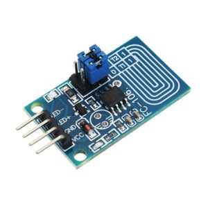
Capacitor Touch Dimmer, Constant Voltage LED Stepless Dimming, PWM Control Board
- Voltage range: 4V to 5V
- Maximum output current: 500mA
- Hole distance: 16 mm
- Aperture: 5 mm
- The lamp brightness can be adjusted by requirement, it is very to operate.
- It can touch in medium protection, such as glass, acrylic, plastic, ceramics, and so on, which is very safe.
- Anti power and phone interference, the EFT can reach above +/-2KV; the touch response sensitivity and reliability will not be affected by the close distance or multi-angle mobile phone interference.
- Dimming mode: Non-polar PWM dimming.
- PCB size: 23 x 20mm


Dual Micro USB 3.7v to 5V 2A Power Bank DIY 18650 LiPo Charger
- 4-level LED lamp display power, not working state intelligent automatic shutdown;
- The built-in lithium battery protection IC, over-current, under-voltage protection;
- Dual USB output ports.
- Dimensions: 68 x 34 x 9 mm (LxWxH)
- Weight: 10 gm
- Input port: MicroUSB (Andro)
- Input requirements: 5V constant voltage power supply can do charge input power, the most matching charger for 5v1a above
- Output port: USB
- Output parameters: 5V1A/5V2A
- Requirements for rechargeable batteries:
- Compatible Batteries: 18650 batteries, cell phone batteries, flat-panel batteries, MP3 batteries, etc. 3.7v-4.2V polymer Lithium battery,

HX711–24 Bit Analog to Digital Converter (ADC)
- It is an ADC converter with two differential input channels
- An active-low noise PGA is integrated inside the chip which provides the gain of 32, 64 and 128
- It has a power-on-reset capability which simplifies digital interface initialization.
- All controls to the IC are made through the pins. Programming is not needed.
- You can select a data rate of 10SPS or 80SPS at the output.
- Provides simultaneous supply rejection of 50Hz and 60Hz supply.
- Built-in analog power supply regulator
- The voltage supply range is from 2.6V to 5.5V
- The temperature range is from -40 °C to +85℃
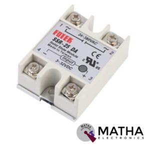
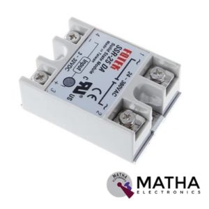
Solid State Relay Module SSR-25DA 25A /250V 3-32V DC Input 24-380VAC Output
- Control mode: DC-AC
- Input voltage: 3-32V DC.
- Output voltage: 24-380V AC.
- Output current: 25A.
- Working voltage: 250V.
- Material: plastic + metal.
- Environment temperature: -30 to +75
- Long service life and high reliability.
- Reduced electromagnetic interference.
- Highly reliable, compact size designed to offer users maximum simplicity.
- Dimension: 6. 5Cm x 4. 5Cm x 2. 2Cm
Reviews
There are no reviews yet.