
I am text block. Click edit button to change this text. Lorem ipsum dolor sit amet, consectetur adipiscing elit. Ut elit tellus, luctus nec ullamcorper mattis, pulvinar dapibus leo.
-50%
33nf 630V DC Polyester Capacitor
Original price was: ₹14.00.₹8.00Current price is: ₹8.00. inc. GST
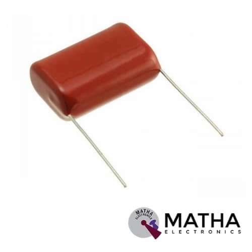
1.5uf 250V DC Polyester Capacitor
Original price was: ₹13.00.₹8.00Current price is: ₹8.00. inc. GST
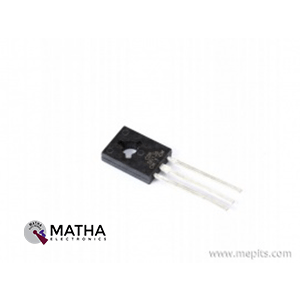
BD139 NPN Transistor 80V 1.5A
Original price was: ₹10.00.₹5.00Current price is: ₹5.00. inc. GST
- Collector-base Voltage: 80V
- Collector Current: 1.5A
- Transistor Polarity: NPN
- Total Power Dissipation: 12.5W
- Current Gain max. : 250
- Package: T0-126
Description
This BD139 NPN bipolar transistor designed explicitly for use in general-purpose low power silicon NPN bipolar junction transistors. The BD139 has a very low saturation voltage and excellent high gain performance. Within the operating range, BD139 is available as a three terminal NPN device. The base current IB determines the collector current IC. For a given collector emitter voltage VCE, every change in the base current causes an amplified change in the collector current.
Transistors are the most important component in an electrical circuit. An NPN transistor is made up of two pieces of P-type silicon (the base) sandwiched between two pieces of N-type silicon (the collector and emitter). These transistors were created with the sole purpose of passing electrons from the emitter to the collector (so conventional current flows from collector to emitter). The emitter “emits” electrons into the base, and the quantity of electrons the emitter emits is controlled by the base. These electrons mix with the holes in the base and are delivered to the collector. The collector “collects” the majority of the electrons released and transmits them to the next portion of the circuit.
The purpose of the NPN transistor is to amplify weak signals that enter the base and create powerful amplify signals at the collector end. The travel of an electron in an NPN transistor is from the emitter to the collector area, resulting in current in the transistor. Because the bulk of charge carriers in such transistors are electrons, which have a higher mobility than holes, they are commonly utilised in circuits. The emitter, collector, and base of an NPN transistor are the three terminals. The centre part of an NPN transistor is weakly doped, and it is the most critical factor in the transistor’s operation. Meanwhile, the emitter was little doped, whereas the collector was extensively doped.
Reviews (0)
Shipping & Delivery

Related products


ADXL 335 Accelerometer IC
- 3-axis sensing
- Small, low profile package
- 4 mm × 4 mm × 1.45 mm LFCSP
- Low power : 350 μA (typical)
- Single-supply operation: 1.8 V to 3.6 V
- 10,000 g shock survival
- Excellent temperature stability
- BW adjustment with a single capacitor per axis
- RoHS/WEEE lead-free compliant
- 8V- 3.6V single-supply operation
- Integrated X, Y, and Z axis accelerometer on a single chip
- X and Y axis has a 0.5Hz to 1600Hz bandwidth
- Z axis has a 0.5Hz to 550Hz bandwidth
- Hermetically sealed for temp and humidity resistance
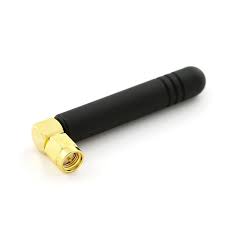
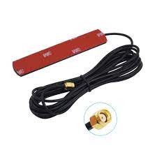
GSM Antenna Dlenp 2dbi/3dbi Patch Antenna with SMA Male Connector
- GSM Antenna
- Gain: 2 to 3dbi
- Wire Length: 3 metre
- 3dbi Sticker Antenna
- GSM Antenna
- SMA Male Connector
- Frequency Range(MHz): 824-960/1710-1990Mhz
- Bandwidth (MHz): 136/280
- VSWR≤1.5
- Gain(dB): 2-3dbi
- Max Input power(W): 60W
- Input Impedance: 50 Ω
- Polarization Type: Vertical
- Cable Type: RG174
- Mounting Adhesive
- Net weight: 47g
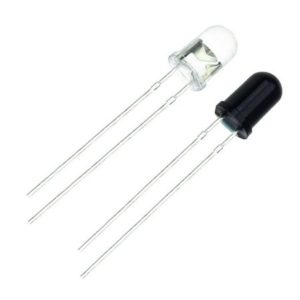
IR LED Sensor
- Size: 5mm LED
- Wavelength: 940nm wavelength (most commonly used)
- Forward current (IF) is 100mA (normal condition) and 300mA (max.)
- 5A of surge forward current
- 24v to 1.4v of forward voltage
- Temperature : -40 to 100 ℃
- Soldering Temperature should not exceed 260 ℃
- Power Dissipation of 150mW at 25℃ (free-air temperature) or below
- Spectral bandwidth of 45nm
- Viewing angle: 30 to 40 degree
- High Reliability
- Excessive radiant intensity
- Having lead spacing of 2.54mm
- Easy to use with breadboard or perf board

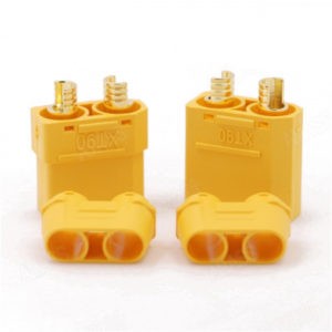
Reviews
There are no reviews yet.