
I am text block. Click edit button to change this text. Lorem ipsum dolor sit amet, consectetur adipiscing elit. Ut elit tellus, luctus nec ullamcorper mattis, pulvinar dapibus leo.
-20%

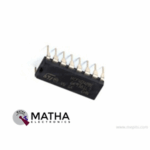
CD4042 Quad Clocked D Latch IC
Original price was: ₹24.00.₹18.00Current price is: ₹18.00. inc. GST
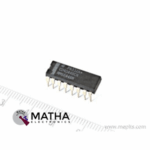
CD4044 CMOS Quad 3-State RS Latch IC
Original price was: ₹21.00.₹15.00Current price is: ₹15.00. inc. GST
CD4043 CMOS Quad 3-State RS Latch IC
Original price was: ₹25.00.₹20.00Current price is: ₹20.00. inc. GST
- CMOS Quad 3-State R/S Latch
- Number of Circuits: 1
- Logic Type: CMOS
- Logic Family: CD4000
- Polarity: Non-Inverting
- Number of Output Lines: 4
- High Level Output Current: – 4.2 mA
- Propagation Delay Time: 350 ns at 5 V, 175 ns at 10 V, 120 ns at 15 V
- Package: PDIP 16
- Supply Voltage Range: 3 to 15 V
- Operating Temperature Range: -55 C to 125 C
Description
CD4043 designed quad cross-coupled 3-STATE CMOS NOR latches. That means it has four R-S latches, all of which are created using the CMOS NOR logical gate. All four latches share a same 3-STATE ENABLE input. Each latch in the IC has its own Q output as well as its own SET and RESET inputs. A single ENABLE input controls all of the Q outputs. The latch states are connected to the Q outputs via a logic “1” or high on the ENABLE input. The latch states are also disconnected from the Q outputs when the ENABLE input is set to logic “0” or low. As a result, an open circuit feature is created, allowing the outputs to be shared. In the meanwhile, this IC has a number of advantages, including good noise immunity, ESD protection, and great thermal overload protection. Meanwhile, the DC Supply Voltage Range (VDD) of the CD4043 is -0.5V to +18V.
An SR latch, also known as an SR Flip-Flop, is a logic circuit with two inputs (S and R) and two outputs (Q and Q’). The status of output Q determines the state of this latch. When Q is 1 (High), the latch is said to be SET, and when Q is 0 (Low), the latch is said to be RESET. Two cross-coupled NAND gates or two cross-coupled NOR gates are used to create an SR latch or flip flop.
Application
- Multiple bus storage
- Strobed register
- Four bits of independent storage with output enable
- General digital logic
Reviews (0)
Shipping & Delivery

Related products


ADXL 335 Accelerometer IC
- 3-axis sensing
- Small, low profile package
- 4 mm × 4 mm × 1.45 mm LFCSP
- Low power : 350 μA (typical)
- Single-supply operation: 1.8 V to 3.6 V
- 10,000 g shock survival
- Excellent temperature stability
- BW adjustment with a single capacitor per axis
- RoHS/WEEE lead-free compliant
- 8V- 3.6V single-supply operation
- Integrated X, Y, and Z axis accelerometer on a single chip
- X and Y axis has a 0.5Hz to 1600Hz bandwidth
- Z axis has a 0.5Hz to 550Hz bandwidth
- Hermetically sealed for temp and humidity resistance
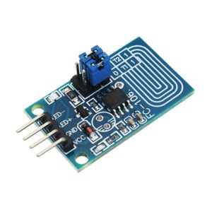
Capacitor Touch Dimmer, Constant Voltage LED Stepless Dimming, PWM Control Board
- Voltage range: 4V to 5V
- Maximum output current: 500mA
- Hole distance: 16 mm
- Aperture: 5 mm
- The lamp brightness can be adjusted by requirement, it is very to operate.
- It can touch in medium protection, such as glass, acrylic, plastic, ceramics, and so on, which is very safe.
- Anti power and phone interference, the EFT can reach above +/-2KV; the touch response sensitivity and reliability will not be affected by the close distance or multi-angle mobile phone interference.
- Dimming mode: Non-polar PWM dimming.
- PCB size: 23 x 20mm


Dual Micro USB 3.7v to 5V 2A Power Bank DIY 18650 LiPo Charger
- 4-level LED lamp display power, not working state intelligent automatic shutdown;
- The built-in lithium battery protection IC, over-current, under-voltage protection;
- Dual USB output ports.
- Dimensions: 68 x 34 x 9 mm (LxWxH)
- Weight: 10 gm
- Input port: MicroUSB (Andro)
- Input requirements: 5V constant voltage power supply can do charge input power, the most matching charger for 5v1a above
- Output port: USB
- Output parameters: 5V1A/5V2A
- Requirements for rechargeable batteries:
- Compatible Batteries: 18650 batteries, cell phone batteries, flat-panel batteries, MP3 batteries, etc. 3.7v-4.2V polymer Lithium battery,

HX711–24 Bit Analog to Digital Converter (ADC)
- It is an ADC converter with two differential input channels
- An active-low noise PGA is integrated inside the chip which provides the gain of 32, 64 and 128
- It has a power-on-reset capability which simplifies digital interface initialization.
- All controls to the IC are made through the pins. Programming is not needed.
- You can select a data rate of 10SPS or 80SPS at the output.
- Provides simultaneous supply rejection of 50Hz and 60Hz supply.
- Built-in analog power supply regulator
- The voltage supply range is from 2.6V to 5.5V
- The temperature range is from -40 °C to +85℃

Reviews
There are no reviews yet.