
I am text block. Click edit button to change this text. Lorem ipsum dolor sit amet, consectetur adipiscing elit. Ut elit tellus, luctus nec ullamcorper mattis, pulvinar dapibus leo.
-29%

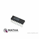
CD4043 CMOS Quad 3-State RS Latch IC
Original price was: ₹25.00.₹20.00Current price is: ₹20.00. inc. GST
7412N Triple 3-Input Positive NAND Gate IC
Original price was: ₹20.00.₹15.00Current price is: ₹15.00. inc. GST
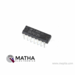
CD4044 CMOS Quad 3-State RS Latch IC
Original price was: ₹21.00.₹15.00Current price is: ₹15.00. inc. GST
- CMOS Quad 3-State RS Latch
- Number of Circuits: 1
- Logic Type: CMOS
- Logic Family: CD4000
- Polarity: Non-Inverting
- Number of Input Lines/Output Lines: 8/4
- High Level Output Current: – 4.2 mA
- Propagation Delay Time: 350 ns at 5 V, 175 ns at 10 V, 120 ns at 15 V
- Supply Voltage Range: 3 to 15V
- Operating Temperature Range: – 55 C to + 125 C
- Package: PDIP 16
Description
CD4044 designed quad cross-coupled 3-STATE CMOS NAND latches. That mean it comes with four R-S latches, made by using the CMOS NAND logical gate. There exist a common 3-STATE ENABLE input for all four latches. Each latch in the IC consists of a separate Q output and individual SET and RESET inputs. The Q outputs controlled via a common ENABLE input. A logic “1” or high on the ENABLE input connects the latch states to the Q outputs. And also a logic “0” or low on the ENABLE input disconnects the latch states from the Q outputs. This results in an open circuit feature that allow common busing of the outputs. Meanwhile, this IC has many features such as high noise immunity, ESD barring, and excellent thermal overload protection. Meanwhile, CD4044 operates at a DC Supply Voltage Range, (VDD) f -0.5V to +18V.
An SR latch, also known as an SR Flip-Flop, is a logic circuit with two inputs (S and R) and two outputs (Q and Q’). The status of output Q determines the state of this latch. When Q is 1 (High), the latch is said to be SET, and when Q is 0 (Low), the latch is said to be RESET. Two cross-coupled NAND gates or two cross-coupled NOR gates are used to create an SR latch or flip flop.
Application
- Multiple bus storage
- Strobed register
- Four bits of independent storage with output enable
- General digital logic
Reviews (0)
Shipping & Delivery

Related products


1/4W 5% Assorted Value Carbon Film Resistor Assortment Kit Set pack electronic diy kit
- 100% brand new and high quality.
- Fine workmanship and long service life.
- 1/4W carbon film resistor package.
- High precision and stability.
- Easy to use.
- Precision: 5%
- Error: 5%
- Values
- 10Ω, 15Ω, 22Ω, 33Ω, 47Ω, 68Ω, 100Ω, 220Ω, 330Ω, 470Ω, 1k, 1k5, 2k2, 3k3, 4k7, 5k6, 6K8, 8K2, 10K, 15K, 22K, 33K, 47K, 56K, 68K, 100K, 150K, 220K, 330K, 470K
- Package included: 150pcs

10 Segment Led Bargraph Light Display Red, Yellow, Green, Blue
- LED type: LED array bar
- Segments: 10
- LED Colour: Green
- Housing color: white
- Reverse voltage: 5V
- Forward Voltage - Typical: 1.85 V
- Forward Voltage - Maximum: 2.2 V
- DC forward current: 30mA
- Peak forward current: 175mA
- Power dissipation: 75mW
- Peak wavelength: 590nm
- Luminous Intensity Typical: 120 Mcd
- Operating temperature: -40°C to +85°C
- 10 Separately Controlled LED's
- High Brightness
- High-Intensity Green Output
- Ideal for Audio and Meter Displays
- Economically priced
- Easy to Mount


5-36v Switch Drive High-power MOSFET Trigger Module
- Operating Voltage: DC 5V - 36V;
- The trigger source: digital high-low (DC3.3V - 20V), can be connected microcontroller IO port, PLC interfaces, DC power, you can access the PWM signal, the signal frequency 0--20KHZ perfect support.
- Output capacity: DC 5V - 36V, at room temperature, continuous current 15A, power 400W! Lower auxiliary cooling conditions, the maximum current up to 30A.
- Applications: You can control the output of power equipment, motors, light bulbs, LED lights, DC motors, micro-pumps, solenoid valves, etc.. You can enter
- PWM, motor speed control, lamp brightness.
- Availability: unlimited switch
- Operating temperature: -40-85
- Dimension: 34mm x 17mm x 12mm
- The use of imported dual-MOS parallel active output, lower resistance, more current, strong power at room temperature, 15A, 400W, to meet the most use of the equipment
- Wide voltage, the perfect support for PWM
- Easily control high power devices
- Input PWM to achieve motor speed control, lamp brightness control

ADXL 335 Accelerometer IC
- 3-axis sensing
- Small, low profile package
- 4 mm × 4 mm × 1.45 mm LFCSP
- Low power : 350 μA (typical)
- Single-supply operation: 1.8 V to 3.6 V
- 10,000 g shock survival
- Excellent temperature stability
- BW adjustment with a single capacitor per axis
- RoHS/WEEE lead-free compliant
- 8V- 3.6V single-supply operation
- Integrated X, Y, and Z axis accelerometer on a single chip
- X and Y axis has a 0.5Hz to 1600Hz bandwidth
- Z axis has a 0.5Hz to 550Hz bandwidth
- Hermetically sealed for temp and humidity resistance
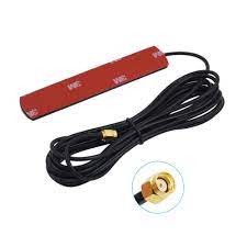
GSM Antenna Dlenp 2dbi/3dbi Patch Antenna with SMA Male Connector
- GSM Antenna
- Gain: 2 to 3dbi
- Wire Length: 3 metre
- 3dbi Sticker Antenna
- GSM Antenna
- SMA Male Connector
- Frequency Range(MHz): 824-960/1710-1990Mhz
- Bandwidth (MHz): 136/280
- VSWR≤1.5
- Gain(dB): 2-3dbi
- Max Input power(W): 60W
- Input Impedance: 50 Ω
- Polarization Type: Vertical
- Cable Type: RG174
- Mounting Adhesive
- Net weight: 47g

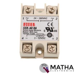
Solid State Relay Module DC To AC SSR-40DA 3-32VDC/24-380VAC 40A
- Control mode: DC-AC
- Input voltage: 3-32V DC.
- Output voltage: 24-380V AC.
- Output current: 40A.
- Working voltage: 250V.
- Material: plastic + metal.
- Loading current: 40A
- Control current: 3-25mA DC
- On voltage: ≤1.5V AC
- One-off Time: ≤10ms
- Off Leakage Current: ≤2mA
- Dielectrics voltage-resistance: 2500VAC
- Environment temperature: -30 to +75
- Long service life and high reliability.
- Reduced electromagnetic interference.
- Highly reliable, compact size designed to offer users maximum simplicity.
Reviews
There are no reviews yet.