
I am text block. Click edit button to change this text. Lorem ipsum dolor sit amet, consectetur adipiscing elit. Ut elit tellus, luctus nec ullamcorper mattis, pulvinar dapibus leo.
-9%
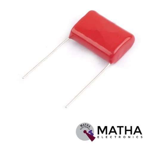
1.5uf 630V DC Polyester Capacitor
Original price was: ₹22.00.₹15.00Current price is: ₹15.00. inc. GST

MIP2C4 Power Device IC
Original price was: ₹75.00.₹65.00Current price is: ₹65.00. inc. GST
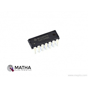
MC1496PG Balanced Modulator Demodulator IC
Original price was: ₹53.00.₹48.00Current price is: ₹48.00. inc. GST
- Balanced Modulator/Demodulator
- Differential Input Signal: 5V
- Maximum Bias Current: 10mA
- Carrier Suppression: 65dB
- Input Bias Current Max: 30µA
- Input Offset Current Max: 7µA
- Output Offset Current Max: 80µA
- Power Dissipation: 33mW
- Package: DIP-14
Description
The MC1496PG Balanced Modulator Demodulator IC is designed for applications where the output voltage is the result of a combination of an input voltage (signal) and a switching function (carrier). It may be used for suppressed carrier and amplitude modulation, synchronous detection, FM detection, phase detection, and chopper applications, among other things. An upper quad differential amplifier is powered by a normal differential amplifier with twin current sources in this design. The output collectors are cross coupled, allowing for full wave balanced multiplication of the two input voltages. That is, the output signal is the product of the two input signs multiplied by a constant.
For the carrier and signal voltage levels provided, carrier suppression is defined as the ratio of each sideband output to carrier output. It is very reliant on the carrier input level. Low carrier values don’t fully switch the upper switching devices, resulting in reduced signal gain and, as a result, lesser carrier suppression. A higher than optimal carrier level causes unnecessary device and circuit carrier feedthrough, causing the suppression figure to degenerate once again. A 60 mVrms sinewave carrier input signal was used to characterize the MC1496. This level is often chosen for balanced modulator applications because it gives the best carrier suppression at carrier frequencies around 500 kHz.
The MC1496 requires three externally controlled dc bias voltage values. Maintaining at least 2.0 V collector base bias on all transistors while not exceeding the voltages shown in the absolute maximum rating table are guidelines for setting up these three levels.
- 30 Vdc >= [(V6, V12) − (V8, V10)] >=2 Vdc
- 30 Vdc >= [(V8, V10) − (V1, V4)] >=2.7 Vdc
- 30 Vdc >= [(V1, V4) − (V5)] >=2.7
Reviews (0)
Shipping & Delivery

Related products


ADXL 335 Accelerometer IC
- 3-axis sensing
- Small, low profile package
- 4 mm × 4 mm × 1.45 mm LFCSP
- Low power : 350 μA (typical)
- Single-supply operation: 1.8 V to 3.6 V
- 10,000 g shock survival
- Excellent temperature stability
- BW adjustment with a single capacitor per axis
- RoHS/WEEE lead-free compliant
- 8V- 3.6V single-supply operation
- Integrated X, Y, and Z axis accelerometer on a single chip
- X and Y axis has a 0.5Hz to 1600Hz bandwidth
- Z axis has a 0.5Hz to 550Hz bandwidth
- Hermetically sealed for temp and humidity resistance

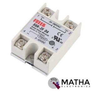
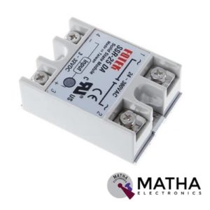
Solid State Relay Module SSR-25DA 25A /250V 3-32V DC Input 24-380VAC Output
- Control mode: DC-AC
- Input voltage: 3-32V DC.
- Output voltage: 24-380V AC.
- Output current: 25A.
- Working voltage: 250V.
- Material: plastic + metal.
- Environment temperature: -30 to +75
- Long service life and high reliability.
- Reduced electromagnetic interference.
- Highly reliable, compact size designed to offer users maximum simplicity.
- Dimension: 6. 5Cm x 4. 5Cm x 2. 2Cm
Reviews
There are no reviews yet.