
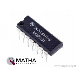
74LS107 Dual J-K Flip-Flop IC

CD4013 Dual D-type Flip-Flop IC
- Dual D-type Flip-Flop
- Supply Voltage: 3 to 20V
- Input Current: ± 10 mA
- Power Dissipation: 200mW
- Low level Output Voltage: 0.05V
- High level Output Voltage min.: 4.95V
- Low level Input Voltage Max.: 1.5V
- High level Input Voltage Min.: 3.5V
- Propagation Delay Time Max.: 400ns
- Maximum Clock Frequency: 24MHz
- Package: DIP-14
CD4099 8-Bit Addressable Latch IC
- 8 Bit Addressable Latch
- Supply Voltage Range: 3 to 20V
- Input Current: ±10mA
- Power Dissipation : 200mW
- Quiescent Current Max. : 100µA
- Low level Output Voltage: 0.05V
- High-level Output Voltage Min.: 4.95V
- Low level Input Voltage Max.: 1.5V
- High level Input Voltage Min.: 3.5V
- Propagation Delay Time Max.: 450ns
- Package: DIP-16

CD4000 Dual 3-Input NOR Gate Plus Inverter IC

CD4072 Dual 4 Input OR Gate IC

CD4073 Triple 3 Input AND Gate IC

74LS253 Dual 4-Line to 1-Line Data Selector Multiplexer IC
- Permits multiplexing from N lines to 1 line
- Performs at parallel-to-serial conversion
- Strobe (enable) line provided for cascading (N lines to n lines)
- High fan-out, low impedance, totem pole outputs
- Typical average propagation delay times From data 14 ns From strobe 19 ns From select 22 ns
- Typical power dissipation 31 mW

74LS251 Data Selector or Multiplexer IC With 3-State Output
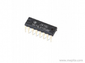
74LS195 Universal 4-Bit Shift Register IC
- Universal 4-Bit Shift Register
- Power Supply Current: 21mA
- Input clamp voltage: -1.5V
- Maximum clock frequency: 25MHz
- Propagation delay time max: 26ns
- Supply voltage range: 4.75 to 5.25V
- Synchronous, Expandable Shift Right
- Synchronous Shift Left Capability
- Synchronous Parallel Load
- Separate Shift and Load Clock Inputs
- Input Clamp Diodes Limit High Speed Termination Effects
- Package: DIP-16
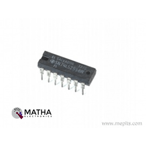
74LS295 4-Bit Right-Shift Left-Shift Register IC
- 4-Bit Right-Shift Left-Shift Register with 3-State Outputs
- High-level input voltage: 2V
- Low-level input voltage: 0.8V
- High-level output voltage: 3.1V
- Low-level output voltage: 0.25V
- Input clamp voltage: -1.5V
- Maximum clock frequency: 45MHz
- Propagation delay time max: 30ns
- Supply voltage range: 4.75 to 5.25V
- Package: DIP-14

74LS299 8-Bit Universal Shift Storage Register IC
- 8-Bit Universal Shift/Storage Register
- High-level input voltage: 2V
- Low-level input voltage: 0.8V
- High-level output voltage: 3.4V
- Low-level output voltage: 0.5V
- Maximum clock frequency: 70MHz
- Propagation delay time max: 24ns
- Power Dissipation: 700mW
- Supply voltage range: 4.75 to 5.25V
- Multiplexed Input/Outputs for Data Hold, Shift Right, Shift Left, and Load Data
- Operates with Outputs Enabled or at High impedance
- Common I/O for Reduced Pin Count
- Four Operation Modes: Shift Left, Shift Right, Load and Store
- Separate Shift Right Serial Input and Shift Left Serial Input for Easy Cascading
- 3-State Outputs Drive Bus Lines Directly
- Can be Cascaded for N-Bit Word Lengths
- Standard TTL Switching Voltages
- Package: DIP-20
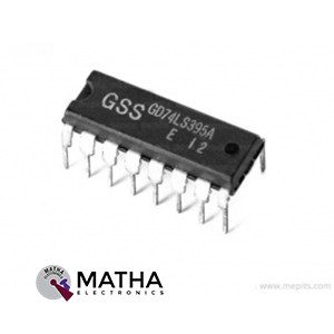
74LS395 4 Bit Cascadable Shift Register IC
- 4 Bit Cascadable Shift Register With 3 State Outputs
- Supply Voltage Range: 4.75V to 5.25V
- Supply Current Max.: 31mA
- Clock Frequency Max.: 45MHz
- HIGH Level Input Voltage Min.: 2V
- LOW Level Input Voltage Max.: 0.8V
- HIGH Level Output Voltage Min.: 2.4V
- LOW Level Output Voltage Max.: 0.4V
- High level Output Current Max.: -2.6mA
- Low level Output Current Max.: 24mA
- Input Clamp Voltage Max.: -1.5V
- Propagation Delay Time Max.: 35ns
- Package: DIP-16