
I am text block. Click edit button to change this text. Lorem ipsum dolor sit amet, consectetur adipiscing elit. Ut elit tellus, luctus nec ullamcorper mattis, pulvinar dapibus leo.
-33%
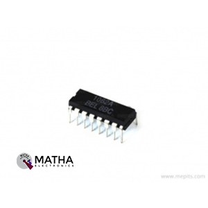
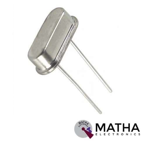
10 MHz 2 Pin Oscillator Crystal
Original price was: ₹13.00.₹8.00Current price is: ₹8.00. inc. GST
UM93214A 1-memory Tone Pulse Dialer IC
Original price was: ₹65.00.₹40.00Current price is: ₹40.00. inc. GST
TEA1062A Low Voltage Transmission Circuits with Dialer Interface IC
Original price was: ₹30.00.₹20.00Current price is: ₹20.00. inc. GST
- Low Voltage Transmission Circuits with Dialer Interface
- Line Voltage: 4V
- Internal Supply Current Max: 1.35mA
- Microphone Amplifier Voltage Gain: 52dB
- Receiving Amplifier Voltage Gain: 31dB
- Common Mode Rejection Ratio (Mic): 82dB
- Package: DIP-16
</div>
Description
The TEA1062A is an integrated circuit that performs all voice and line interface tasks in fully electronic telephone systems. These gadgets are designed to transition between dialling and speaking via electrical switching. To allow for the usage of several telephone sets linked in parallel, the ICs function at line voltages as low as 1.6 V DC (with decreased performance.
The telephone line provides the power necessary for the IC and its peripheral circuitry. The IC regulates the supply voltage, which is obtained from the line through a dropping resistor. External circuits, such as dialling and control circuits, are likewise powered by the supply voltage VCC. A capacitor between VCC and VEE is used to decouple the supply voltage. A capacitor between REG and VEE decouples the internal voltage regulator. Meanwhile, the exchange supply voltage Vexch, the feeding bridge resistance Rexch, and the DC resistance of the telephone line Rline define the DC current flowing into the set.
A 3.6 k resistor connected between STAB and VEE controls the amount of the circuit’s inbuilt current stabiliser (see Fig.9). The surplus current is shunted to VEE through LN when the line current (Iline) is more than 0.5 mA larger than the total of the IC supply current (ICC) and the current drawn by peripheral circuitry linked to VCC (Ip). Calculate the regulated voltage on the line terminal (VLN) as follows:
VLN = Vref + ISLPE × R9
VLN = Vref + {(Iline − ICC − 0.5 × 10⁻³ A) − Ip} × R9
Vref is an internally generated temperature compensated reference voltage of 3.7 V and R9 is an external resistor connected between SLPE and VEE.
Reviews (0)
Shipping & Delivery

Related products

5-36v Switch Drive High-power MOSFET Trigger Module
- Operating Voltage: DC 5V - 36V;
- The trigger source: digital high-low (DC3.3V - 20V), can be connected microcontroller IO port, PLC interfaces, DC power, you can access the PWM signal, the signal frequency 0--20KHZ perfect support.
- Output capacity: DC 5V - 36V, at room temperature, continuous current 15A, power 400W! Lower auxiliary cooling conditions, the maximum current up to 30A.
- Applications: You can control the output of power equipment, motors, light bulbs, LED lights, DC motors, micro-pumps, solenoid valves, etc.. You can enter
- PWM, motor speed control, lamp brightness.
- Availability: unlimited switch
- Operating temperature: -40-85
- Dimension: 34mm x 17mm x 12mm
- The use of imported dual-MOS parallel active output, lower resistance, more current, strong power at room temperature, 15A, 400W, to meet the most use of the equipment
- Wide voltage, the perfect support for PWM
- Easily control high power devices
- Input PWM to achieve motor speed control, lamp brightness control

650NM Laser Diode
- Wavelength: 650nm
- Output optical power: 5mW
- Operating voltage: 5V
- Operating current: ~30mA
- Input current: 30mA
- Housing material: Copper
- Power lead length: 120mm.
- Transmit power: 58mW
- Spot: size 10mm to 15mm at 15meters
- Life span more than 2000 hours
- Driver circuit: APC circuit
- Small size
- Cost-effective
- Breadboard friendly
- Operating temperature -10°C to 40°C
- Dimension: :15mm x 6mm
- Weight: 10 grams


ADXL 335 Accelerometer IC
- 3-axis sensing
- Small, low profile package
- 4 mm × 4 mm × 1.45 mm LFCSP
- Low power : 350 μA (typical)
- Single-supply operation: 1.8 V to 3.6 V
- 10,000 g shock survival
- Excellent temperature stability
- BW adjustment with a single capacitor per axis
- RoHS/WEEE lead-free compliant
- 8V- 3.6V single-supply operation
- Integrated X, Y, and Z axis accelerometer on a single chip
- X and Y axis has a 0.5Hz to 1600Hz bandwidth
- Z axis has a 0.5Hz to 550Hz bandwidth
- Hermetically sealed for temp and humidity resistance
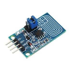
Capacitor Touch Dimmer, Constant Voltage LED Stepless Dimming, PWM Control Board
- Voltage range: 4V to 5V
- Maximum output current: 500mA
- Hole distance: 16 mm
- Aperture: 5 mm
- The lamp brightness can be adjusted by requirement, it is very to operate.
- It can touch in medium protection, such as glass, acrylic, plastic, ceramics, and so on, which is very safe.
- Anti power and phone interference, the EFT can reach above +/-2KV; the touch response sensitivity and reliability will not be affected by the close distance or multi-angle mobile phone interference.
- Dimming mode: Non-polar PWM dimming.
- PCB size: 23 x 20mm
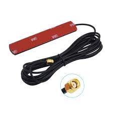
GSM Antenna Dlenp 2dbi/3dbi Patch Antenna with SMA Male Connector
- GSM Antenna
- Gain: 2 to 3dbi
- Wire Length: 3 metre
- 3dbi Sticker Antenna
- GSM Antenna
- SMA Male Connector
- Frequency Range(MHz): 824-960/1710-1990Mhz
- Bandwidth (MHz): 136/280
- VSWR≤1.5
- Gain(dB): 2-3dbi
- Max Input power(W): 60W
- Input Impedance: 50 Ω
- Polarization Type: Vertical
- Cable Type: RG174
- Mounting Adhesive
- Net weight: 47g

HX711–24 Bit Analog to Digital Converter (ADC)
- It is an ADC converter with two differential input channels
- An active-low noise PGA is integrated inside the chip which provides the gain of 32, 64 and 128
- It has a power-on-reset capability which simplifies digital interface initialization.
- All controls to the IC are made through the pins. Programming is not needed.
- You can select a data rate of 10SPS or 80SPS at the output.
- Provides simultaneous supply rejection of 50Hz and 60Hz supply.
- Built-in analog power supply regulator
- The voltage supply range is from 2.6V to 5.5V
- The temperature range is from -40 °C to +85℃

Reviews
There are no reviews yet.