

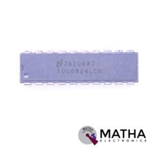
PCF8583 IC
- I2C-bus interface operating supply voltage: 2.5 V to 6 V
- Clock operating supply voltage 1.0 V to 6.0 V at 0 Cto+70C
- 240 8-bit low-voltage RAM
- Data retention voltage: 1.0 V to 6.0 V
- Operating current (at fSCL = 0 Hz): max 50 μA
- Clock function with four year calendar
- Universal timer with alarm and overflow indication
- 24 hour or 12 hour format
- 32.768 kHz or 50 Hz time base
- Serial input and output bus (I2C-bus)
- Automatic word address incrementing
- Programmable alarm, timer, and interrupt function
- Slave addresses: A1h or A3h for reading, A0h or A2h for writing
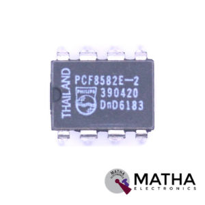
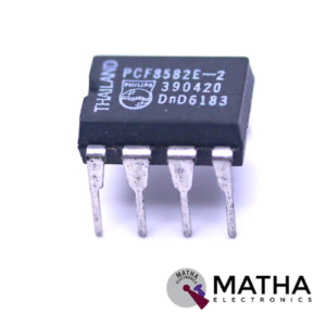
PCF8582E-2 IC DIP-8
- Low power CMOS
- Non-volatile storage of 2 kbits organized as 256 × 8-bit
- Single supply with full operation down to 2.5 V
- On-chip voltage multiplier
- Serial input/output I2C-bus
- Write operations:
- - byte write mode
- Read operations:
- Internal timer for writing (no external components)
- Internal power-on reset
- 0 kHz to 100 kHz clock frequency
- High reliability by using a redundant storage code


IC PT2399 SMD


IC PT2322
- 6-Channel Audio Processor IC
- Very Low Power Consumption (DC=9V)
- I2C Bus Control
- 6-Channel Individual Input
- 6-Channel Master Volume Control: 0 to -79 dB (1 dB/step)
- 6-Channel Individual Output TRIM Volume Control: 0 to -15 dB (1dB/step)
- 3-Band Tone Control (Treble, Middle, Bass): + 14dB , 2dB/step
- Mute Function
- 3D Effect Function
- Tone Defeat Function
- Low Noise
- High Channel Separation
- Low Harmonic Distortion
- Least External Components
- Package: SO-28


IC PT2314 SMD
- 4 stereo inputs with gain selection, range from 0dB to +11.25dB in 3.75dB/step
- Master volume from 0 dB to -78.75dB in 1.25dB/step
- Speaker attenuator for balance, range from 0dB to -38.75dB in 1.25dB/step
- Each channel output can be muted individually.
- Low frequency loudness compensation
- Bass and Treble control, range from -14dB to +14dB in 2dB/step
- Wide operation range (VDD=4V to 10V)
- Low harmonic distortion, low noise
- Improved and replace PT2314 and PT2314A
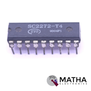
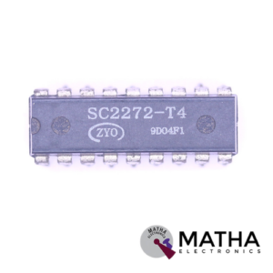
PT2272 IC

IC PT2258 SMD
- CMOS Technology
- Mounting type: SMD
- Low Power Consumption
- Least External Components
- Attenuation Range: 0 to -79dB at 1dB/step
- Operating Voltage: 5 to 9 V
- Low Noise, S/N Ratio>100dB (A-weighting)
- High Channel Separation
- I2C Bus Control Interface
- Selectable Address
- 6-Channel Outputs
- Available in 20 pins, DIP or SOP

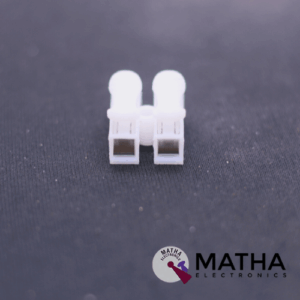
2 Way 5A Wire Connector

3 Way 5A Wire Connector


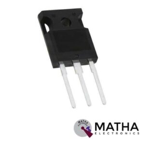
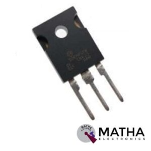
Mosfet 15R1203
- Function : 1200V, 15A
- Reverse conducting IGBT / Reverse conducting IGBT
- Package: TO-247-3 Type
- Powerful monolithic body diode with a low forward voltage
- Designed for soft commutation only
- very tight parameter distribution
- high ruggedness, temperature stable behavior
- low VCEsat
- easy parallel switching capability due to positive
- temperature coefficient in VCEsat
- Low EMI
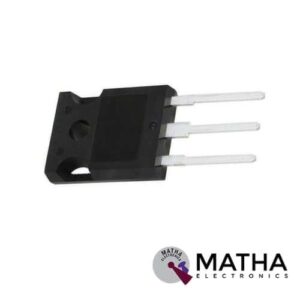
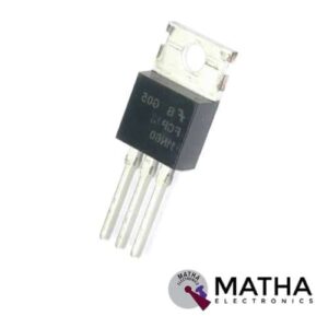
Mosfet 10N90 Big
- Type Designator: 10N90
- Type of Transistor: MOSFET(Big)
- Type of Control Channel: N -Channel
- Maximum Power Dissipation (Pd): 183 W
- Maximum Drain-Source Voltage |Vds|: 900 V
- Maximum Gate-Source Voltage |Vgs|: 30 V
- Maximum Drain Current |Id|: 10 A
- Maximum Junction Temperature (Tj): 150 °C
- Rise Time (tr): 54 nS
- Drain-Source Capacitance (Cd): 245 pF
- Maximum Drain-Source On-State Resistance (Rds): 1.15 Ohm
- Package: TO-247 TO-3P
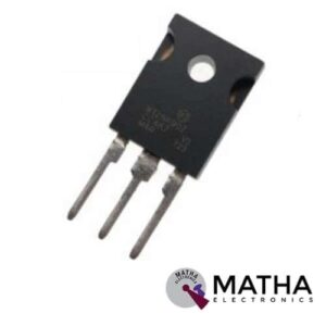
Mosfet 12N60
- 12N60 is the type designation.
- MOSFET is the transistor type used in the 12N60.
- N-Channel is the type of control channel.
- W: 225 Maximum power dissipation (Pd)
- |Uds| maximum drain-source voltage, V: 600
- Maximum drain current |Id|, A: 12 Maximum gate-source voltage |Ugs|, V: 30
- Maximum junction temperature (Tj), in degrees Celsius: 150
- 12N60 transistor rise time (tr), nS: 115
- Capacitance at the drain (Cd), pF: 200
- Maximum on-state drain-source resistance (Rds), Ohm: 0.6
Mosfet 11N60 Small
- Type Designator: 11N60
- Type of Transistor: MOSFET(Big)
- Type of Control Channel: N -Channel
- Maximum Drain-Source Voltage |Vds|: 650 V
- Maximum Drain Current |Id|: 11 A
- Maximum Junction Temperature (Tj): 150 °C
- Extremely low gate charge (often Qg=40nC)
- A low effective output capacitance (typical Coss.eff=95pF)
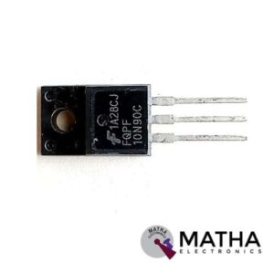
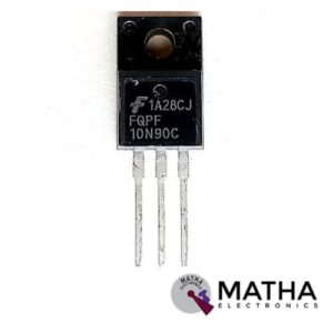
Mosfet 10N90
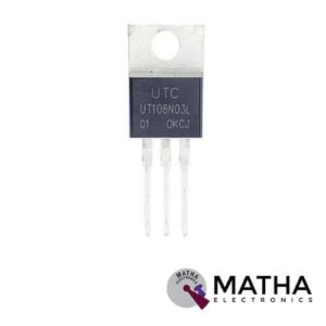
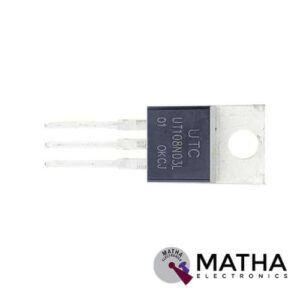
Mosfet 108N03
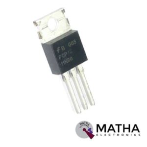
Mosfet 105N03
- Type of Transistor: MOSFET
- Type of Control Channel: N -Channel
- Maximum Power Dissipation (Pd): 140 W
- Maximum Drain-Source Voltage |Vds|: 30 V
- Maximum Gate-Source Voltage |Vgs|: 20 V
- Maximum Gate-Threshold Voltage |Vgs(th)|: 2.5 V
- Maximum Drain Current |Id|: 150 A
- Maximum Junction Temperature (Tj): 175 °C
- Total Gate Charge (Qg): 42 nC
- Rise Time (tr): 91 nS
- Drain-Source Capacitance (Cd): 400 pF
- Maximum Drain-Source On-State Resistance (Rds): 0.0035 Ohm
- Package: TO-220
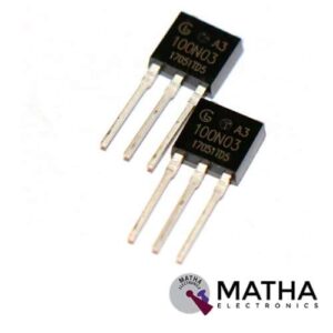
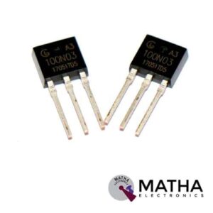
Mosfet 100N03 SMD
- Type of Transistor: MOSFET
- Type Designator:100N03
- Type of Control Channel: N -Channel
- Maximum Drain-Source Voltage:30 V
- Maximum Gate-Source Voltage:20 V
- Maximum Drain Current:100 A
- Drain-Source Capacitance:1300 pF
- Maximum Operating Junction Temperature:175 °C
- Maximum Drain-Source On-State Resistance:0.0055 Ohm
- Maximum Power Dissipation:180 W
- Package: TO220
- Simple Drive Requirement
- Low Gate Charge
- Fast Switching
- RoHS Compliant
- High cell density for ultra-low RdsonAvalanche voltage and current are fully characterized.