
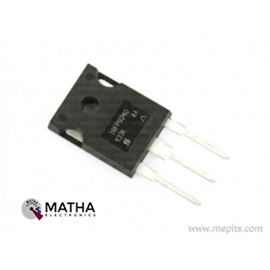
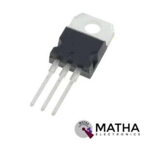
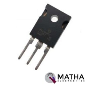
IRFP9240 P-Channel Power Mosfet Transistor -200V -12A
- P-Channel Power Mosfet
- Drain Current: ID= -12A at TC=25℃
- Drain Source Voltage: VDS = -200V
- Static Drain-Source On-Resistance: RDS(on) < 500mΩ
- Power Dissipation: 150W
- Package: TO-247AC
- Dynamic dV/dt Rating
- Repetitive Avalanche Rated
- Isolated Central Mounting Hole
- Fast Switching
- Ease of Paralleling
- Simple Drive Requirements
- Lead (Pb)-free Available
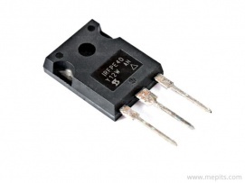
IRFPE40 Power Mosfet Transistor 800V 5.4A

IRFZ44N Power Mosfet Transistor 55V 49A

IRFZ48N Power Mosfet Transistor 55V 64A
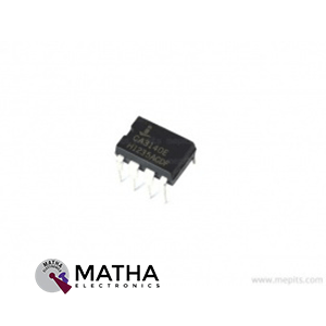
LF351 Wide Bandwidth JFET Input Operational Amplifier IC
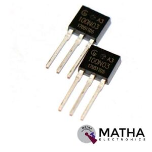
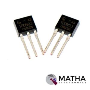
Mosfet 100N03 SMD
- Type of Transistor: MOSFET
- Type Designator:100N03
- Type of Control Channel: N -Channel
- Maximum Drain-Source Voltage:30 V
- Maximum Gate-Source Voltage:20 V
- Maximum Drain Current:100 A
- Drain-Source Capacitance:1300 pF
- Maximum Operating Junction Temperature:175 °C
- Maximum Drain-Source On-State Resistance:0.0055 Ohm
- Maximum Power Dissipation:180 W
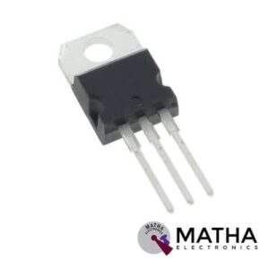
- Package: TO220
- Simple Drive Requirement
- Low Gate Charge
- Fast Switching
- RoHS Compliant
- High cell density for ultra-low RdsonAvalanche voltage and current are fully characterized.
Mosfet 105N03
- Type of Transistor: MOSFET
- Type of Control Channel: N -Channel
- Maximum Power Dissipation (Pd): 140 W
- Maximum Drain-Source Voltage |Vds|: 30 V
- Maximum Gate-Source Voltage |Vgs|: 20 V
- Maximum Gate-Threshold Voltage |Vgs(th)|: 2.5 V
- Maximum Drain Current |Id|: 150 A
- Maximum Junction Temperature (Tj): 175 °C
- Total Gate Charge (Qg): 42 nC
- Rise Time (tr): 91 nS
- Drain-Source Capacitance (Cd): 400 pF
- Maximum Drain-Source On-State Resistance (Rds): 0.0035 Ohm
- Package: TO-220
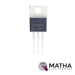
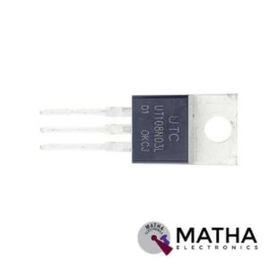
Mosfet 108N03
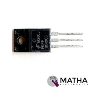
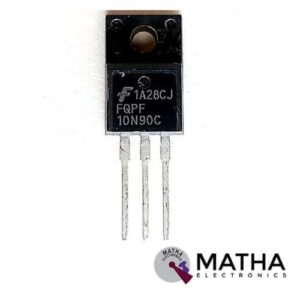
Mosfet 10N90
Mosfet 10N90 Big
- Type Designator: 10N90
- Type of Transistor: MOSFET(Big)
- Type of Control Channel: N -Channel
- Maximum Power Dissipation (Pd): 183 W
- Maximum Drain-Source Voltage |Vds|: 900 V
- Maximum Gate-Source Voltage |Vgs|: 30 V
- Maximum Drain Current |Id|: 10 A
- Maximum Junction Temperature (Tj): 150 °C
- Rise Time (tr): 54 nS
- Drain-Source Capacitance (Cd): 245 pF
- Maximum Drain-Source On-State Resistance (Rds): 1.15 Ohm
- Package: TO-247 TO-3P
Mosfet 11N60 Small
- Type Designator: 11N60
- Type of Transistor: MOSFET(Big)
- Type of Control Channel: N -Channel
- Maximum Drain-Source Voltage |Vds|: 650 V
- Maximum Drain Current |Id|: 11 A
- Maximum Junction Temperature (Tj): 150 °C
- Extremely low gate charge (often Qg=40nC)
- A low effective output capacitance (typical Coss.eff=95pF)

Mosfet 12N60
- 12N60 is the type designation.
- MOSFET is the transistor type used in the 12N60.
- N-Channel is the type of control channel.
- W: 225 Maximum power dissipation (Pd)
- |Uds| maximum drain-source voltage, V: 600
- Maximum drain current |Id|, A: 12 Maximum gate-source voltage |Ugs|, V: 30
- Maximum junction temperature (Tj), in degrees Celsius: 150
- 12N60 transistor rise time (tr), nS: 115
- Capacitance at the drain (Cd), pF: 200
- Maximum on-state drain-source resistance (Rds), Ohm: 0.6